Graphenea launches $99 miniGFET fully-packaged devices
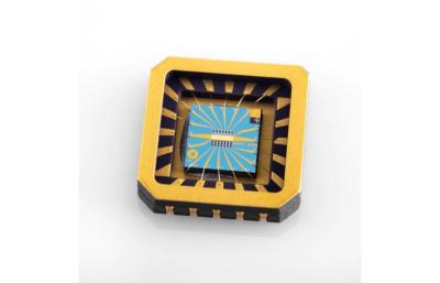
Graphenea launched two new products out of its Graphene Foundry, which they call mGFET or miniGFET. These are Graphenea's highest value-chain products, which are manufactured and packaged in chip carriers, and can be used together with the freshly released Graphenea Card for seamless sensor development.

The mGFET is available from $99, and as it is a fully-package device, it is ready to be integrated into standard electronics. Order volume can range from a few devices for early prototyping, to JEDEC trays with hundreds of devices which are compatible with automated pick & place routines.
International collaboration conducts comparison of Raman spectroscopic analysis of CVD-grown graphene
The results of an international comparison of the measurement of graphene, led by NPL, have been released. The work was conducted through the Versailles Project on Advanced Materials and Standards (VAMAS) and in collaboration with institutes from around the world.
The international interlaboratory comparison (ILC) outlined improvements that reduce measurement uncertainty, in some cases by a factor of 15, and which will be the basis for a new international standard which is currently under development within ISO/IEC for Raman spectroscopy. This will aim to become a verified source of data and ultimately provide more accurate and precise measurement standards for the global graphene industry.
Graphenea Foundry launches new GFET process
This is a sponsored post by Graphenea
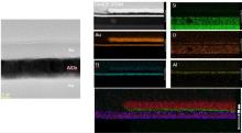
Graphenea has announced that, following the release of its GFET S30, it has developed a High-K Metal Gate (HKMG) manufacturing process to create Field-Effect Transistor (FET) structures on graphene, or GFETs. This process is now available under the dedicated GFAB service, starting February 2022.

HKMG structures triggered a revolution in Si electronics when they were introduced during the early 2000’s, creating an alternative to SiO2 gate dielectrics that paved the way for further scaling. HKMG technology indeed enabled Moore’s law to continue, providing increased capacitance and lower current leakage than the previously state-of-the-art SiO2 tech. The most common FET architecture to modulate the conductance in graphene uses a SiO2 gate dielectric grown on top of a heavily doped Si substrate. Whereas this structure is easy to implement, it suffers from excessive current leakage when the SiO2 layer is thinned down, often rendering devices unusable. Moreover, the substrate acts as a global backgate, forbidding manipulation of individual GFET devices, which is essential for many applications.
Graphenea launches Cartridge S2X for easy fabrication of graphene-based sensors
Graphenea has released a new product intended to make sensing with graphene easier: The Cartridge S2X, a package that interfaces the graphene microdevice and the electrical equipment used for its readout.

The cartridge has a small cleft onto which to place the GFET die, just below the electronics module with gentle pogo contacts to the graphene chip. The contacts are placed for seamless integration with Graphenea's S20, S21, S20P and S21P graphene chips that are especially designed for biosensing. The design makes use of 8 connections to the chip, including six source electrodes, one drain, and one gate. The pins are routed to a standard 8-pin BNC connector, for an easy and robust link to external measurement equipment.
Graphenea certified for medical device components
This is a sponsored post by Graphenea
Graphenea has obtained ISO 13485 certification for manufacturing medical device components. The certification relates to the GFET product line and the Graphene Foundry service.

The ISO standard is an important certification needed for the commercialization of medical applications of graphene, in particular non-implantable biosensors. Graphenea obtained certification for the entire process chain, including raw materials, design, development, manufacture and sale. The certificate also applies to facilities, quality management, tracing, and data analysis. The ISO certificate was issued after an independent audit by SGS.
Graphenea Foundry: a platform for the manufacture of graphene-based devices
This is a sponsored post by Graphenea
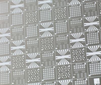
Graphenea’s Semiconductor catalogue spans from 1x1 cm2 single layer graphene films on a variety of substrates, to fully customized graphene-based device architectures implemented on wafers up to 150mm. The unique vertical integration that Graphenea offers, that covers the graphene growth, its transfer, its device fabrication and post-processing, allows Graphenea to have full control of the manufacturing process, continuously monitoring this through quality control processes and checkpoints.

Graphenea Foundry offers three products and services, which cover all the graphene needs one may have.
New project aims to turn urban waste into graphene and other useful materials
Graphenea will be taking part in a flagship project called CIRCULAR BIOCARBON, which was kicked off this week and has been awarded over â¬23 Million, to develop a first-of-its kind flagship biorefinery designed to turn the organic fraction of municipal solid waste (OFMSW) and sewage sludge (SS) into added-value products, from mechanical moving parts, to night vision cameras and devices for 5G telecommunications.
The project, which received full marks from the European Commission, involves 11 partners from five European countries (including Spain, Italy, Denmark, France and Germany) and is a milestone for the whole Europe owing to its implementation scale (industrial level) as well as to its replicability potential.
Terahertz imaging of graphene could promote industrialization
A collaborative team of Graphene Flagship partners from DTU, Denmark, IIT, Italy, Aalto University, Finland, AIXTRON, UK, imec, Belgium, Graphenea, Spain, Warsaw University, Poland, and Thales R&T, France, as well as collaborators in China, Korea and the US, has come together to develop and mature terahertz spectroscopy techniques, that can penetrate graphene films and enable the creation of detailed maps of their electrical quality, without damaging or contaminating the material. The result of this collaborating is a novel measurement tool for graphene characterization.
Graphene is often ‘sandwiched’ between many different layers and materials to be used in electronic and photonic devices, which complicates the process of quality assessment. Terahertz spectroscopy can help by imaging the encapsulated materials and revealing the quality of the graphene underneath, exposing imperfections at critical points in the fabrication process. It is a fast, non-destructive technology that probes the electrical properties of graphene and layered materials, with no need for direct contact.
Graphenea now offers custom graphene oxide dispersions
Graphenea recently introduced a new service for the graphene industry, a custom  graphene oxide (GO) dispersion service. This service provides researchers with an opportunity to receive GO in a solvent and at a concentration which is most compatible with their application.
According to Graphenea, its GO is noted for its mechanical and thermal properties, in addition to having a high monolayer content (>95%). This service not only offers researchers the option of receiving GO in water at a custom concentration, but also GO dispersed into: Acetone, DMF, DMSO, Ethanol, IPA, Methanol, NMP, Tetra butyl-acetate, or Toluene.
The first International Graphene Awards winners are announced
The International Graphene Awards (IGA) was initiated by the Chinese Graphene Industry Association (CGIA) in collaboration with 50 graphene experts from all over the world.
In 2020 the IGA committee offered 5 different awards: for best graphene products, best graphene firm, industry promotion, industry demonstration and honorary award for the most contribution people in graphene industry.
Pagination
- Previous page
- Page 2
- Next page