Electronics - Page 7

Researchers develop simple method to achieve fine control over the integration of foreign atoms into graphene

Researchers from South Korea invented a simple way to achieve fine control over the integration of foreign atoms with graphene, developing composite graphene-based heterostructures that can be used to store energy at low cost and fabricate ultrathin, wearable electronics.

Adding foreign atoms to graphene boosts its properties ןצשעק

One way to specifically tailor graphene's properties is by integrating other materials into it, such as metals, insulators, and semiconductors, to form composite structures with desirable properties. For instance, researchers are adding metal oxides to graphene to create graphene monolayer/metal-oxide nanostructures (GML/MONSs) that have improved physical and chemical properties. However, depositing uniform layers of metal oxides over graphene without disturbing the characteristics of the graphene layer is extremely challenging.
Read the full story Posted: Sep 05,2021

Researchers experiment with LIG to create improved wearable health devices

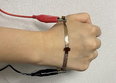
A Penn State-led international research team (led by Professor Huanyu Larry Cheng at Penn State) recently published two studies that could boost research and development of future motion detection, tactile sensing and health monitoring devices.

Graphene made with lasers for wearable health devices image

There are various substances that can be converted into carbon to create graphene through laser radiation, in a process called laser-induced graphene (LIG). The resulting product can have specific properties determined by the original material. The team set out to test this process and has reached interesting conclusions.

Read the full story Posted: Sep 04,2021

Boron nitride assists in protecting graphene in order to achieve next-gen electronics

Researchers from AMO, Oxford Instruments, Cambridge University, RWTH Aachen University and the University of Wuppertal have demonstrated a new method to use plasma enhanced atomic layer deposition (PEALD) on graphene without introducing defects into the graphene itself.

Currently, the most advanced technique for depositing dielectrics on graphene is atomic layer deposition (ALD), which allows to precisely control the uniformity, the composition and the thickness of the film. The process typically used on graphene and other 2D materials is thermal water-based ALD, as it does not damage the graphene sheet. However, the lack of nucleation sites on graphene limits the quality of the dielectric film, and requires the deposition of a seed layer prior to ALD to achieve good results. Another approach is plasma enhanced atomic layer deposition (PEALD), which, when applied to growth on graphene, can introduce surface damage. This is what to team addressed in this recent work.

Read the full story Posted: Aug 09,2021

Researchers develop graphene aerosol gel inks for printing micro-supercapacitors

Researchers from Kansas State University, led by Suprem Das, assistant professor of industrial and manufacturing systems engineering, in collaboration with Christopher Sorensen, university distinguished professor of physics, have shown potential ways to manufacture graphene-based nano-inks for additive manufacturing of supercapacitors in the form of flexible and printable electronics.

The team’s work could be adapted to integrate supercapacitors to overcome the slow-charging processes of batteries. Furthermore, Das has been developing additive manufacturing of small supercapacitors — called micro-supercapacitors — so that one day they could be used for wafer-scale integration in silicon processing.

Read the full story Posted: Jul 30,2021

Researchers show that stretching can change the electronic properties of graphene

A research team led by the University of Basel has found that the electronic properties of graphene can be specifically modified by stretching the material evenly.

The researchers, led by Professor Christian Schönenberger at the Swiss Nanoscience Institute and the Department of Physics at the University of Basel, have studied how the material’s electronic properties can be manipulated by mechanical stretching. In order to do this, they developed a kind of rack by which they stretch the atomically thin graphene layer in a controlled manner, while measuring its electronic properties.

Read the full story Posted: Jun 29,2021

Cardea Bio partners with Scentian Bio to create a bio-electronic tongue/nose platform

Cardea Bio, a biotech company integrating molecular biology with semiconductor electronics, has signed a commercial partnership with Scentian Bio. Scentian is an expert in synthetic insect odorant receptors (iORs), one of nature’s ways of detecting and interpreting smells.

The partnership will enable Scentian to use a customized Cardean chipset, built with graphene-based biology-gated transistors, which will allow Scentian to manufacture a bio-electronic tongue/nose tech platform.

Read the full story Posted: May 18,2021

Researchers design atomically precise graphene nanoribbon heterojunction sensor

An international research team, led by the University of Cologne, has succeeded in connecting several atomically precise graphene nanoribbons to form complex structures. The scientists have synthesized and spectroscopically characterized nanoribbon heterojunctions, and were able to integrate the heterojunctions into an electronic component. In this way, they have created a novel sensor that is highly sensitive to atoms and molecules.

"The graphene nanoribbon heterojunctions used to make the sensor are each seven and fourteen carbon atoms wide and about 50 nanometres long. What makes them special is that their edges are free of defects. This is why they are called "atomically precise" nanoribbons," explained Dr. Boris Senkovskiy from the Institute for Experimental Physics. The researchers connected several of these nanoribbon heterojunctions at their short ends, thus creating more complex heterostructures that act as tunneling barriers.

Read the full story Posted: May 16,2021

Rice team modifies laser-induced graphene process to create micron-scale patterns in photoresist

A Rice University team has modified its laser-induced graphene technique to make high-resolution, micron-scale patterns of the conductive material for consumer electronics and other applications. Laser-induced graphene (LIG), introduced in 2014 by Rice chemist James Tour, involves burning away everything except carbon from polymers or other materials, leaving the carbon atoms to reconfigure themselves into films of characteristic hexagonal graphene. The process employs a commercial laser that writes graphene patterns into surfaces that to date have included wood, paper and even food.

Rice lab uses laser-induced graphene process to create micron-scale patterns in photoresist image

The new version writes fine patterns of graphene into photoresist polymers, light-sensitive materials used in photolithography and photoengraving. Baking the film increases its carbon content, and subsequent lasing solidifies the robust graphene pattern, after which unlased photoresist is washed away.

Read the full story Posted: May 07,2021

Duke team creates fully recyclable printed electronics

Researchers at Duke University have created transistors with three carbon-based inks. The all-carbon thin-film transistors were made using crystalline nanocellulose as a dielectric, carbon nanotubes as a semiconductor, graphene as a conductor and paper as a substrate. This type of component could assist in addressing the environmental problem of accumulation of electronics that are non-recyclable.

Silicon-based computer components are probably never going away and we don’t expect easily recyclable electronics like ours to replace the technology and devices that are already widely used, said Professor Aaron Franklin, an electrical engineer at Duke University. But we hope that by creating new, fully recyclable, easily printed electronics and showing what they can do, that they might become widely used in future applications.

Read the full story Posted: Apr 28,2021

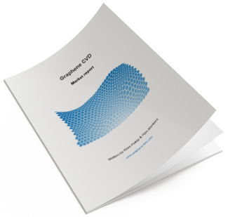
Introducing: The CVD Graphene Market Report

Graphene-Info is proud to present our new market report, The CVD Graphene Market Report. This market report, brought to you by the world's leading graphene industry experts, is a comprehensive guide to CVD graphene materials, the current industry and market status, and the promising applications in optoelectronics, bio-sensors, thermal solutions and more.

Reading this report, you'll learn all about:

  • How does CVD graphene differ from other graphene types
  • CVD graphene properties
  • Possible applications for CVD graphene
  • Available materials on the market

The report also provides a list of prominent CVD graphene research activities, a list of all CVD graphene developers and their products, datasheets and brochures from over 10 different CVD graphene makers and more.

Read the full story Posted: Mar 24,2021