Researchers develop method for optimizing both the growth and the transfer process of graphene
A team of researchers from the University of Cambridge, RWTH Aachen University and the National Institute for Materials Science in Japan has developed a methodology for simultaneously optimizing the growth and the transfer process of graphene, showing that it is possible to dry-transfer graphene with high-yield, if the crystallographic orientation of the growth surface is chosen appropriately.
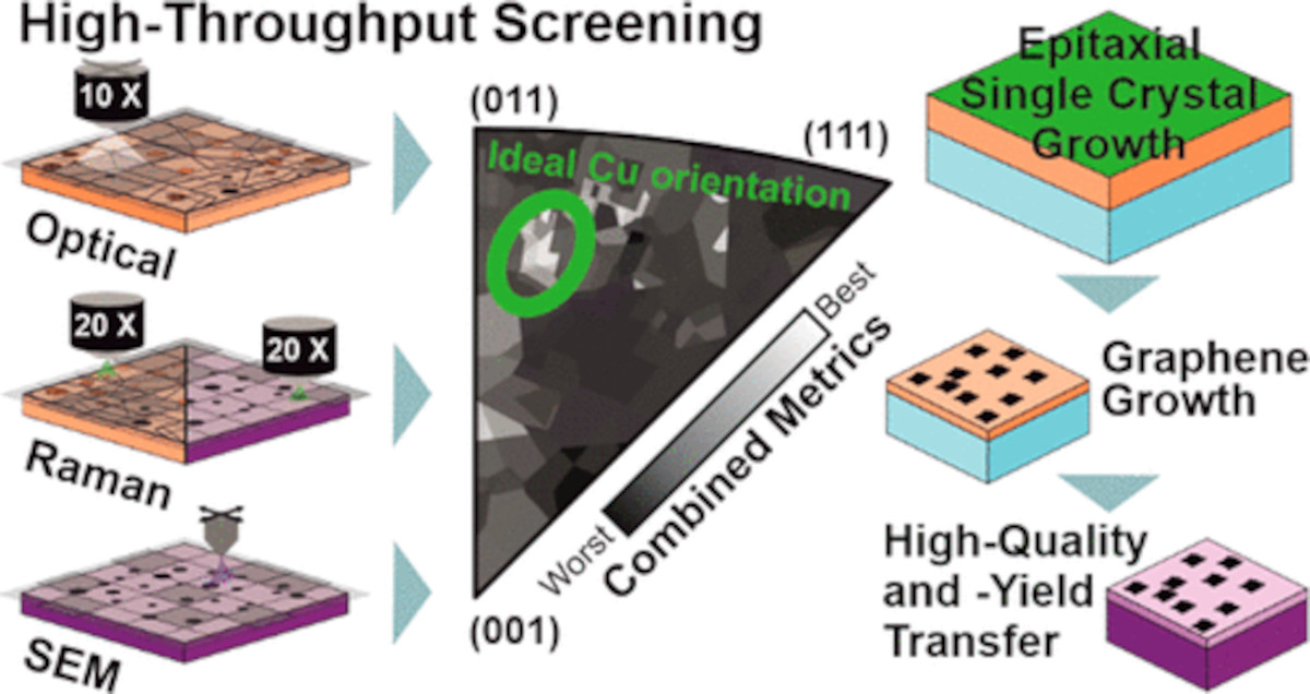
Graphene often needs to be transferred from the growth substrate (typically copper) to a final substrate where components can be built. However, current transfer approaches either lead to a substantial degradation of the crystal quality or are not compatible with high-volume manufacturing. Moreover, while graphene has great potential for next generation electronics, the gap between the performance of “hero devices” realized in research labs and what can be reproducibly fabricated with scalable approaches remains large. This is why high-end electronic devices enabled by graphene are still not on the market – and why scalability is such a challenge in terms of making the most of this nanomaterial.