Graphene-Info | Graphene industry portal - Page 3

Graphene experiment proves patterns in chaos in quantum realm

Researchers from the University of California, Harvard University, University of Manchester, UC Santa Cruz and the National Institute for Materials Science in Tsukuba, Japan have conducted an experiment that confirms a 40 year old theory that electrons confined in quantum space would move along common paths rather than producing a chaotic array of trajectories.

Electrons exhibit both particle and wave-like properties and behave in ways that are often counterintuitive, and under certain conditions, their waves can interfere with each other in a way that concentrates their movement into certain patterns. Physicists call these common paths “unique closed orbits.”

Read the full story Posted: Dec 05,2024

New collaboration will develop microscopy techniques for imaging chemical reactions at the atomic scale

Scientists from the University of Illinois Chicago (UIC), University of Chicago, University of Illinois Urbana-Champaign and Argonne National Laboratory are collaborating on new electron microscopy techniques to allow the imaging of chemical reactions at the atomic scale. The Center for Multimodal Observations for Single Atom Imaging of Chemistry, or MOSAIC, was funded this fall through a $1.8 million grant from the National Science Foundation. 

The collaboration, part of the NSF Centers for Chemical Innovation program, will create “liquid cells” that allow scientists to set up, control and measure chemical reactions under a microscope. The researchers will use powerful, state-of-the-art electron microscopes at UIC to capture these reactions in motion, providing fresh insight into atomic and molecular dynamics.

Read the full story Posted: Dec 04,2024

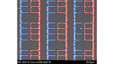
Researchers use graphene in novel technique for self-assembling electronics

Researchers from North Carolina State University and Iowa State University have demonstrated a new technique for self-assembling electronic devices. The proof-of-concept work was used to create diodes and transistors, and could pave the way for self-assembling more complex electronic devices without relying on existing computer chip manufacturing techniques.

D-Met fabricated patterns produce components for potential use in microelectromechanical systems (MEMS). Image credit: Julia Chang and NCSU.

“Existing chip manufacturing techniques involve many steps and rely on extremely complex technologies, making the process costly and time consuming,” says Martin Thuo, corresponding author of a paper on the work and a professor of materials science and engineering at North Carolina State University. “Our self-assembling approach is significantly faster and less expensive. We’ve also demonstrated that we can use the process to tune the bandgap for semiconductor materials and to make the materials responsive to light – meaning this technique can be used to create optoelectronic devices. What’s more, current manufacturing techniques have low yield, meaning they produce a relatively large number of faulty chips that can’t be used. Our approach is high yield – meaning you get more consistent production of arrays and less waste.”

Read the full story Posted: Dec 04,2024

Haydale reports its latest financial results for its Fiscal Year 2024

Haydale has announced its financial results for Q3 2024, which is the end of its 2024 fiscal year. Haydale says that while it has developed an excellent pipeline of opportunities, the timeline of converting these into sales takes longer than anticipated.

Haydale's revenue in FY2024 was 4.82 million GBP (up 12% from 2023), and the company reported a slightly improved loss of 3.16 million GBP (down from 3.49 million in 2023).

Read the full story Posted: Dec 03,2024

Sparc Technologies reports significant performance improvements achieved in graphene hnhanced water-based coatings

Sparc Technologies has announced the results of initial test work in water-based acrylic epoxy coatings. The testing has reportedly demonstrated significant corrosion performance improvements through the incorporation of low dosages of carefully selected grades of graphene compared to an unmodified control. Testing has been performed using two industry-recognized electrochemical measurement techniques.

Water-based coatings are gaining prominence due to better environmental credentials compared to more widely used solvent-based coatings which contain fossil fuel derived organic solvents. These results are the first evidence that Sparc has seen whereby graphene significantly improves the corrosion performance of water-based coatings. This extends Sparc’s reach into a new and rapidly growing area of the coatings market where there are clear performance challenges to address. It also complements Sparc’s flagship ecosparc® product range.

Read the full story Posted: Dec 03,2024

Graphene transistors could enable ultrasensitive detection of infections

Researchers from Friedrich Schiller University Jena, CNM Technologies, NOXXON Pharma, APTARION Biotech and Radboud University Medical Center have developed graphene field effect transistor (GFET) sensors based on van der Waals (vdW) heterostructures of single-layer graphene layered with a molecular ≈1 nm thick carbon nanomembrane (CNM).


1 / 1Schematic illustration of the fabrication steps of the l-AP/PEG-CNM GFET sensors. Credit: Advanced Materials 

The CNM acts as an ultrathin molecular interposer between the graphene channel and the analyte and allows bio-functionalization without impairing the graphene properties including its charge carrier mobility. 

Read the full story Posted: Nov 29,2024

Adisyn acquires 2D Generation to bring graphene into advanced semiconductors

Israeli-based 2D Generation (2DG), which specializes in graphene-based solutions for semiconductors, has been acquired by ASX-listed Adisyn (ASX:AI1), a provider of tech services for SMEs in the Australian defense sector that has expanded its focus to the semiconductor industry through this acquisition.


Adisyn is also one of the founders of Connecting Chips European Union Joint Undertaking, a collaboration that includes industry leaders like NVIDIA, Valeo, and Applied Materials. This acquisition not only brings Adisyn cutting-edge technology, but potentially opens the door for the company to enter the semiconductor space.

Read the full story Posted: Nov 28,2024