IBM fabricated a graphene 2-Ghz doubler RF circuit in a CMOS-compatible process

IBM researchers has fabricated a 2-GHz graphene frequency doubler RF circuit in a CMOS-compatible manufacturing process, on 8" wafers. To fabricate this the researchers inverted the usual manufacturing process and define gate structures first on silicon wafers and then transfer graphene layers fabricated using chemical vapor deposition to the silicon. After defining the areas of graphene IBM was able to attach source and drain contacts to the graphene to complete FET structures.

Inverted-T gate structureInverted-T gate structure

The device itself, the frequency doubler, integrates multiple field effect transistors and radio frequency passives and demonstrated a conversion gain of approximately -25db (at 2 Ghz).

Read the full story Posted: Sep 18,2011

New research into how graphene nanoribbons grow from an anthracene polymer on a gold substrate

Researchers from the UK and Sweden have investigated how graphene nanoribbons grow from an anthracene polymer on a gold substrate, using simluations on a supercomputer. They discovered that in the most likely nanoribbon growth process, the gold substrate acts as more than just a support where the reaction can take place. The gold actually catalyzes the reaction.

It turns out that the graphene nanoribbons grow in a way that resembles the domino effect.

Read the full story Posted: Sep 16,2011

Graphite SPL patterning in Gas

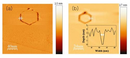
Researchers from the Sejong University in South Korea developed a graphite patterning method based on scanning probe lithography (SPL) - performed in a controlled gas environment. SPL is usually done in air, but this prohibits uniform patterning. The new method could enable better graphite or graphene patterning.

The team reports that methyl alcohol (MA) facilitates graphite etching and gives a line width as narrow as 3 nm. Due to its low surface tension and highly adsorptive behavior, MA provides advantages for narrow line width and high speed etching operation.

Read the full story Posted: Sep 08,2011

Graphene inverters at room temperature

Researchers from Purdue University developed room temperature graphene inverters. They say that these new inverters could enable graphene transistors - which could be used in all sorts of digital applications.


The new inverters has a gain factor above one - an essential condition if you want to use these in transistors.

Read the full story Posted: Sep 08,2011

Tunable graphene microribbons made to respond to terahertz light

Researchers from Berkeley built a microscale device that responds to light at terahertz frequencies. The device is an array made of graphene microribbons. By varying the width of the ribbons and the concentration of charge carriers in them, the scienstists were able to control the collective oscillations of electrons (plasmons) in the microribbons.

Read the full story Posted: Sep 05,2011

Researchers use metallic NW-graphene (MN-G) hybrid nanostructures for flexible field emission devices

Korean Researchers developed a simple and efficient low-temperature route to prepare metallic nanowires graphene (MN-G) hybrid nanostructures for flexible field emission devices. The idea is to transfer the graphene layer onto an anodic alumina oxide template and then grow vertically aligned gold (Au) nanowires via electrodeposition.

The nanowires length and diameter can be controlled in this method, an also it avoids any high-temperature steps or unconventional lithography procedures. This means that it could be used with flexible and soft substrates. This can lead to completely flexible field emission devices.

Read the full story Posted: Sep 04,2011

MIT opens a center for graphene devices and systems (MIT-CG)

MIT announced the creation of the MIT/MTL Center for Graphene Devices and Systems (MIT-CG). This is an interdepartmental center which is part of the Microsystems Technology Laboratories (MTL) with an aim to bring together MIT researchers and industrial partners to advance the science and engineering of graphene-based technologies.

The MIT-CG will research the basic physical properties of graphene and will also explore advanced technologies and strategies that will lead to graphene-based materials, devices and systems for a variety of applications (including graphene-enabled systems for energy generation, smart fabrics and materials, radio-frequency communications, and sensing).

Read the full story Posted: Sep 02,2011

Hybrid silicon-graphene flash memory outperforms regular flash chips

Researchers from Samsung and the University of California developed a new Flash memory device that integrates both Silicon and Graphene. The idea is to use graphene as the storage layer - which extends the capabilities of the conventional silicon based technology. The new prototypes use less energy and store data more stably over time.

The graphene memory cells also do not electrically interfere with one another, which means that it'll be easier to scale these cells and make them smaller than regular flash cells.

Read the full story Posted: Sep 02,2011

New efficient epitaxy-based method to produce graphene

Dr. Wlodzimierz Strupinski from the Institute of Electronics Materials Technology says that he developed an efficient and cheap method of harvesting Graphene, using commercially available equipment. The new method relies on the crystallization of carbon from an outer source, which means the carbon is settled down in the form of a one or two atom thick layer on the surface. That's an adaptation of an existing process called epitaxy, which may lead to commercial scale production - as he uses standard commercial machinery.

Read the full story Posted: Sep 01,2011