This is a sponsored post by Graphenea
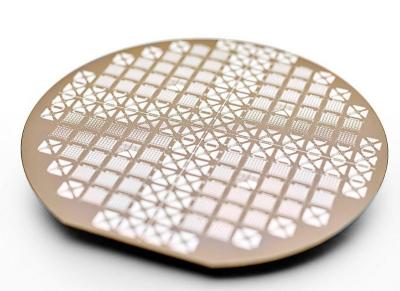
Graphenea has announced that, following the release of its GFET S30, it has developed a High-K Metal Gate (HKMG) manufacturing process to create Field-Effect Transistor (FET) structures on graphene, or GFETs. This process is now available under the dedicated GFAB service, starting February 2022.

HKMG structures triggered a revolution in Si electronics when they were introduced during the early 2000’s, creating an alternative to SiO2 gate dielectrics that paved the way for further scaling. HKMG technology indeed enabled Moore’s law to continue, providing increased capacitance and lower current leakage than the previously state-of-the-art SiO2 tech. The most common FET architecture to modulate the conductance in graphene uses a SiO2 gate dielectric grown on top of a heavily doped Si substrate. Whereas this structure is easy to implement, it suffers from excessive current leakage when the SiO2 layer is thinned down, often rendering devices unusable. Moreover, the substrate acts as a global backgate, forbidding manipulation of individual GFET devices, which is essential for many applications.
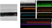
The newly introduced HKMG process by the Graphenea Foundry simultaneously resolves both gate leakage and individual addressing of GFETs, enabling further reliable scaling of devices. Using Aluminum Oxide as gate dielectric, the process enables producers to build FET structures with aggressive dielectric scaling down to an Equivalent Oxide Thickness (EOT) of just 5 nm. Compared to a standard 90 nm SiO2 dielectric, the new technology allows devices to operate under a tenfold reduction in gate voltage, which makes Graphenea’s GFETs more accessible and compatible with a wider range of electronics. This surprisingly also comes with a reduction in leakage current from the nA to the pA range, a 1000x improvement in performance.
In addition to the quantitative benefits described above, the new technology signals a qualitative leap, by enabling local modulation of conductance, for addressing individual devices on a chip. This is of great importance in many applications, especially in optoelectronics and photonics. The HKMG process enables the fabrication of pixelated structures for photodetector arrays, and HKMG structures for electro-optical modulation in waveguides.
These two applications represent the largest technological and business opportunities for graphene in the near future, and both are made available with the HKMG process that Graphenea Foundry is pioneering.
Graphenea Foundry follows a pure-play foundry model. The company makes its customer’s ideas and prototypes a reality, following a unique vertical integration scheme: grow, transfer and process the graphene, all under one roof. This allows Graphenea to monitor the manufacturing process continuosly and deliver high-quality, reliable graphene-based devices, tailored tothe customer's needs. Graphenea Foundry specialises in biosensing and optoelectronic & photonic applications. Graphenea supports its customers with its expertise in graphene manufacturing from early prototyping to commercialisation.
Our range of products and services cover all the Graphene needs one may have:
- GFETs
- Multiproject Wafer Runs
- GFAB (scale-up technology)
- Interfaces
