2D materials

New junction method helps control graphene's properties, could open new paths for next-gen electronics

Researchers at Korea's Pohang University of Science and Technology and Japan's National Institute for Materials Science have developed a way to control the properties of graphene by combining superconductors and graphene. 

Professor Lee Gil-ho of Pohang University of Science and Technology (POSTECH) and researchers from the Research Institute, in collaboration with Kenji Watanabe and Takashi Taniguchi from the National Institute for Materials Science (NIMS) in Japan, noted they have successfully improved the junction characteristics between graphene and superconducting electrodes. 

Read the full story Posted: Dec 31,2024

Researchers gain better understanding of electrons in pentalayer graphene

MIT researchers have gained new understanding of what leads electrons to split into fractions of themselves. Their solution sheds light on the conditions that give rise to exotic electronic states in graphene and other two-dimensional systems.

The recent work attempts to make sense of a discovery that was reported earlier this year by a different group of physicists at MIT, led by Assistant Professor Long Ju. Ju’s team found that electrons appear to exhibit “fractional charge” in pentalayer graphene — a configuration of five graphene layers that are stacked atop a similarly structured sheet of boron nitride.

Read the full story Posted: Nov 24,2024

Researchers develop platform that integrates 2D polaritons with detection system for miniaturized spectrometers

Polaritons are coupled excitations of electromagnetic waves with either charged particles or vibrations in the atomic lattice of a given material. One of their most attractive properties is the capacity to confine light at the nanoscale, which is even more extreme in two-dimensional (2D) materials. 2D polaritons have been investigated by optical measurements using an external photodetector. However, their effective spectrally resolved electrical detection via far-field excitation remains unexplored. This hinders their exploitation in crucial applications such as sensing, hyperspectral imaging, and optical spectrometry, banking on their potential for integration with silicon technologies. 

Recently, researchers from Spain's ICFO, the University of Ioannina, Universidade do Minho, the International Iberian Nanotechnology Laboratory, Kansas State University, the National Institute for Materials Science (Tsukba, Japan), POLIMA (University of Southern Denmark) and URCI (Institute of Materials Science and Computing, have reported on the electrical spectroscopy of polaritonic nanoresonators based on a high-quality 2D-material heterostructure, which serves at the same time as the photodetector and the polaritonic platform. Subsequently, the team electrically detected these mid-infrared resonators by near-field coupling to a graphene pn-junction. The nanoresonators simultaneously exhibited extreme lateral confinement and high-quality factors. 

Read the full story Posted: Oct 23,2024

New spinout called 2D Nano to produce 2D materials sustainably

Imperial College London has spun out a company called 2D Nano, led by Dr. Andrius Patapas, Professor Omar Matar, Professor Camille Petit (Department of Chemical Engineering), and Dr. Jason Stafford (Department of Mechanical Engineering, University of Birmingham), to pioneer the production of advanced materials like graphene, boron nitride, molybdenum disulfide, and more. 

Recently, 2D Nano reportedly secured £2 million in funding from private investors, allowing the Company to scale up production of 2D materials to several tonnes per year. Their internal research and development suggests this can lead to the manufacturing of graphene-enhanced products in excess of 100,000 t/y. The Company is particularly focused on deploying its materials in high-demand sectors such as concrete, coatings, and energy storage, where significant sustainability benefits can be realized. 

Read the full story Posted: Oct 10,2024

New platform allows scientists to study materials at the level of individual molecules

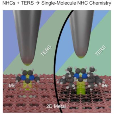
University of Illinois Chicago scientists have created a new platform to study materials at the level of individual molecules. The approach is a significant breakthrough for creating nanotechnologies that could revolutionize computing, energy and other fields.

Two-dimensional materials, such as graphene, are made from a single layer of atoms. Studying and designing these ultrathin materials requires highly specialized methods. The laboratory of Nan Jiang, associate professor of chemistry and physics at UIC, pioneered a new method to simultaneously examine the structural, electronic and chemical properties of these nanomaterials. The platform combines two scientific approaches — scanning probe microscopy and optical spectroscopy — to view materials and assess how they interact with chemicals.

Read the full story Posted: Sep 21,2024

Khalifa University’s RIC2D and LOLC Advanced Technologies Australia advance their partnership

Khalifa University of Science and Technology’s Research & Innovation Center for Graphene and 2D Materials (RIC2D), through its commercial arm spinoff company INTRATOMICS™, and LOLC Advanced Technologies Australia, a subsidiary of the Sri Lanka-based LOLC Group, have announced their collaboration following an agreement on the development of graphene-related products for precision applications.

The joint production of graphene in commercial quantities and development of advanced materials manufacturing marks this phase of the partnership as INTRATOMICS™ and LOLC Advanced Technologies Australia consolidate their roles in this agreement following the earlier MoU signed in August 2023.

Read the full story Posted: Aug 10,2024

Chinese researchers discover naturally occurring few-layer graphene in the Chang’e-5 lunar samples for the first time

Chinese researchers have reportedly discovered naturally occurring few-layer graphene in the lunar samples brought back by the Chang’e-5 probe, which provides new insights into the moon’s geological activities, evolutionary history, and environmental characteristics, broadening understanding of the complex mineral composition of lunar soil and offering information on resource utilization on the moon.

According to the research team from Jilin University, it is estimated that approximately 1.9 percent of the total interstellar carbon exists in the form of graphene, whose morphology and properties are determined by a specific formation process. Therefore, natural graphene can provide important reference and information for the geological evolution of celestial bodies and the in-situ resource utilization on the moon.

Read the full story Posted: Jun 24,2024

Researchers electrically manipulate a ‘chiral interface state’ in a 2D material

Researchers from  Purdue University, University of California, Lawrence Berkeley National Laboratory and Japan's National Institute for Materials Science have managed to electrically manipulate a ‘chiral interface state’ in twisted monolayer-bilayer graphene, with potential for energy-efficient microelectronics and quantum computing.

The international research team, led by Lawrence Berkeley National Laboratory (Berkeley Lab), has taken the first atomic-resolution images and demonstrated electrical control of a chiral interface state – an exotic quantum phenomenon that could help researchers advance quantum computing and energy-efficient electronics.

Read the full story Posted: Apr 11,2024

Researchers use graphene to develop protective layer for 2D quantum materials

Researchers at the Würzburg-Dresden Cluster of Excellence ct.qmat, along with additional collaborators, have developed a graphene-based protective film that shields quantum semiconductor layers just one atom thick from environmental influences without compromising their quantum properties. This could advance the use of these delicate atomic layers in ultrathin electronic components.

A few years ago, scientists from the Cluster of Excellence ct.qmat discovered that topological quantum materials such as indenene hold great promise for ultrafast, energy-efficient electronics. These extremely thin quantum semiconductors are composed of a single atom layer – in indenene’s case, indium atoms – and act as topological insulators, conducting electricity virtually without resistance along their edges. Experimental physicist Professor Ralph Claessen explained that producing such a single atomic layer requires sophisticated vacuum equipment and a specific substrate material. To utilize this two-dimensional material in electronic components, it would need to be removed from the vacuum environment. However, exposure to air, even briefly, leads to oxidation, destroying its revolutionary properties and rendering it useless.

Read the full story Posted: Mar 02,2024

Researchers develop adhesive tape that can transfer 2D materials like graphene in an easier, cheaper and less-damaging way

Researchers from Kyushu University, Nitto Denko Corporation, Tokyo Institute of Technology, Osaka University, National Institute of Advanced Industrial Science and Technology (AIST) and Samsung Electronics have developed a tape that can be used to stick 2D materials to many different surfaces, in an easy and user-friendly way. 

Transfer process of monolayer graphene from Cu(111)/sapphire to a SiO2/Si substrate using the UV tape. Image from Nature Electronics

“Transferring 2D materials is typically a very technical and complex process; the material can easily tear, or become contaminated, which significantly degrades its unique properties,” says lead author, Professor Hiroki Ago of Kyushu University's Global Innovation Center. “Our tape offers a quick and simple alternative, and reduces damage.”

Read the full story Posted: Feb 12,2024