2D materials - Page 8

Graphene-based structures found to have extremely long spin relaxation lifetime

Researchers from Spain's ICN2 institute have discovered that graphene/TMDC heterostructures can exhibit etremely long spin relaxation lifetime. These structure feature lifetimes that are orders of magnitude larger than anything observed in 2D materials - and in fact these results point to a qualitatively new regime of spin relaxation.
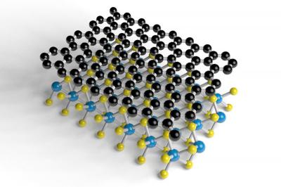
Graphene on TMDC image (ICN2)

Spin relaxation lifetime means that time it takes for the spin of electrons in a spin current to lose their spin (return to the natural random disordered state). A long lifetime is very important for spintronics devices. This new study reveals that the rate at which spins relax in graphene/TMDC systems depends strongly on whether they are pointing in or out of the graphene plane, with out-of-plane spins lasting tens or hundreds of times longer than in-plane spins.

Read the full story Posted: Nov 18,2017

Cambridge University inkjet prints graphene-hBN FETs on textiles

Researchers from Cambridge University have demonstrated how graphene and other related 2D materials (namely hBN) can be directly printed onto textiles to create fully inkjet-printed dielectrically gated field effect transistors (FETs) with solution processed 2D materials.

Cambridge team prints graphene-hbn inks on textiles image

According to the team, these devices are washable, flexible, cheap, safe, comfortable to wear and environmentally-friendly, essential requirements for applications in wearable electronics. The team also demonstrated the first reprogrammable memories, inverters and logic gates with solution processed 2D materials by coupling these FETs together to create integrated circuits, the most fundamental components of a modern-day computer.

Read the full story Posted: Nov 08,2017

Chinese scientists design a flexible graphene-based energy storage membrane

Researchers from Tsinghua University in China have designed a low-cost energy storage device using a TiO2-assisted UV reduction of sandwiched graphene components. The sandwich structure consists of two active layers of reduced graphene oxide hybridized with TiO2, with a graphene oxide separator (rGO-TiO2/rGO/rGO-TiO2). In the device, the separator layer also acts as a reservoir for the electrolyte, which affects ion diffusion—a known problem for layered membrane devices—and affects both the capacity and rate performance.

Graphene flexible supercapacitor membrane process image

The team explained that a step-by-step vacuum filtration process is used to form the membrane structure, and the amount of graphene oxide used in the filtration solutions can be adjusted to precisely tune the thickness of each layer. Irradiation of the dried membrane with UV light then reduces the graphene oxide to rGO with assistance from the TiO2.

Read the full story Posted: Jul 19,2017

Graphene and hBN used to develop a 2D RRAM memory device

Researchers from Soochow University in China developed a 2D RRAM device structure based on sheets of graphene and hexagonal boron nitride (hBN). The device uses a Graphene/hBN/Graphene structure and it features excellent overall fitting results.

2D Graphene / hBN RRAM design

This is still just a theoretical model, but it may prove to be the basis of high performance RRAM devices.

Read the full story Posted: Jun 01,2017

Researchers discover a magnetic 2D material

Researchers from the Lawrence Berkeley National Laboratory discovered the world's first magnetic 2D material - chromium germanium telluride (CGT). It was debatable whether magnetism could survive in such thin materials - and this discovery could pave the way to extremely thin spintronics devices.

Detecting electron spin in CGT, Berkeley

The CGT flakes were produced using the scotch-tape method - the same one used to produce graphene for the first time in Manchester in 2004.

Read the full story Posted: Apr 30,2017

Cambridge team develops a method for producing conductive graphene inks with high concentrations

Researchers at the Cambridge Graphene Centre at the University of Cambridge, UK, have designed a method for producing high quality conductive graphene inks with high concentrations. Conductive inks are useful for a range of applications, including printed and flexible electronics, transistors, and more.

The method uses ultrahigh shear forces in a microfluidization process to exfoliate graphene flakes from graphite. The process is said to convert 100% of the starting graphite material into usable flakes for conductive inks, avoiding the need for centrifugation and reducing the time taken to produce a usable ink. The research also describes optimization of the inks for different printing applications, as well as giving detailed insights into the fluid dynamics of graphite exfoliation.

Read the full story Posted: Feb 22,2017

Graphene Flagship team creates graphene-based quantum LEDs that emit single photons

Researchers from the Graphene Flagship have used layered materials including graphene, boron nitride and a transition metal dichalcogenide (TMD) to create all electrical quantum LEDs which can emit single photons. The devices are said to have the potential to act as on-chip photon sources in quantum information applications.

The LEDs are made of thin layers of different materials, stacked to form a heterostructure. Electrical current is injected into the device, tunnelling from single layer graphene, through a tunnel barrier of a few layers of boron nitride and into a mono- or bilayer of a transition metal dichalcogenide (TMD), such as tungsten diselenide (WSe2). In this layer, electrons recombine with holes to emit single photons.

Read the full story Posted: Sep 26,2016

Graphene enables stretchable reliable memory device for next-gen electronics

Researchers at the Korean IBS, in collaboration with Sungkyunkwan University, have designed a novel graphene-based stretchable and flexible memory device for wearable electronics.

The team has constructed a memory called two-terminal tunnelling random access memory (TRAM), where two electrodes, referred to as drain and source, resemble the two communicating neurons of the synapse in the brain. While mainstream mobile electronics use the so-called three-terminal flash memory, the advantage of two-terminal memories like TRAM is that two-terminal memories do not need a thick and rigid oxide layer. While Flash memory is more reliable and has better performance, TRAM is more flexible and can be scalable, according to the team.

Read the full story Posted: Sep 06,2016

Graphene "balloons" endure extreme pressure and could help evaluate other materials

Researchers at The University of Manchester have shown that small "balloons" made using graphene can endure huge pressures. This could be used to create miniature pressure machines that can withstand massive pressures, and pose a major step towards quickly identifying the way molecules respond under extreme pressure.

The graphene balloons normally form when depositing graphene on flat substrates and are typically thought of as a useless. The researchers at Manchester observed the nano-bubbles closely and discovered that the dimensions and shape of the nano-bubbles offer direct data regarding the elastic strength of graphene as well as its interaction with the underlying substrate. They were able to measure the pressure applied by graphene on a material caught within the balloons, or vice versa.

Read the full story Posted: Aug 26,2016

Researchers model a way to make graphene-like structures from salt

Researchers from Moscow Institute of Physics and Technology (MIPT), in collaboration with researchers from other Russian institutions, have designed a way to acquire 2D graphene-like layers of various rock salts. Thanks to the unique properties of atomically thin materials, this opens up fascinating prospects for nanoelectronics. Based on the computer simulation, they derived the equation for the number of layers in a crystal that will produce ultrathin films with potential applications in nanoelectronics.

Previous theoretical studies suggested that under certain conditions, films with a cubic structure and ionic bonding could spontaneously convert to a layered hexagonal graphitic structure in what is known as graphitisation. However, there was very little experimental data to make any practical use of this proposal.

Read the full story Posted: Aug 10,2016