Band gap

Researchers succeed in creating graphene-based functional semiconductor

Researchers at the Georgia Institute of Technology and China's Tianjin University have created a novel functional semiconductor made from graphene, potentially opening the door to various next-gen electronics. 


This discovery comes at a time when silicon, the material from which nearly all modern electronics are made, is reaching its limit in the face of increasingly faster computing and smaller electronic devices. The semiconductor made from graphene is compatible with conventional microelectronics processing methods – a necessity for any viable alternative to silicon.

Read the full story Posted: Jan 05,2024

Researchers create symmetric graphene quantum dots for future qubits

Researchers from Germany's RWTH Aachen University, Forschungszentrum Jülich and Japan's National Institute for Materials Science (NIMS) have found that bilayer graphene allows the realization of electron–hole double quantum dots that exhibit near-perfect particle–hole symmetry. Moreover, They showed that particle–hole symmetric spin and valley textures lead to a protected single-particle spin-valley blockade that will allow robust spin-to-charge and valley-to-charge conversion, which are essential for the operation of spin and valley qubits.

Quantum dots in semiconductors such as silicon or gallium arsenide are considered great candidates for hosting quantum bits in future quantum processors. The recent study essentially shows that bilayer graphene has even more to offer than other materials. The double quantum dots the researchers have created are characterized by a nearly perfect electron-hole-symmetry that allows a robust read-out mechanism – one of the necessary criteria for quantum computing. 

Read the full story Posted: May 11,2023

International team develops novel method to modify the structure and properties of graphene

An international research team, that included researchers from the Harbin Institute of Technology in China, INRS in France and more, has demonstrated a novel process to modify the structure and properties of graphene. This process relied on a chemical reaction known as photocycloaddition, that modifies the bonds between atoms using ultraviolet (UV) light.

Photocycloaddition of the BCM layer with graphene image

"No other material has properties similar to graphene, yet unlike semiconductors used in electronics, it lacks a band gap. In electronics, this gap is a space in which there are no energy levels that can be occupied by electrons. Yet it is essential for interacting with light," explains Professor Federico Rosei of INRS's Énergie Matériaux Télécommunications Research Centre.

Read the full story Posted: Dec 16,2020

New graphene nanoribbons could enable smaller electronic devices

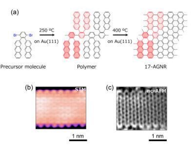
A new collaborative study has reported a 17-carbon wide graphene nanoribbon and found that it has the tiniest bandgap observed so far among familiar graphene nanoribbons prepared through a bottom-up approach.

17-carbon wide graphene nanoribbons to pave the way for new GNR-based electronic devices image(a) Bottom-up synthesis scheme of 17-AGNR on Au(111), (b) high-resolution STM image, and (c) nc-AFM image of 17-AGNR. Image Credit: Junichi Yamaguchi, Yasunobu Sugimoto, Shintaro Sato, Hiroko Yamada.

The study is part of a project of CREST, JST Japan including Nara Institute of Science and Technology (NAIST), the University of Tokyo, Fujitsu Laboratories and Fujitsu.

Read the full story Posted: Jul 06,2020

Graphene-based platform could selectively identify deadly strains of bacteria

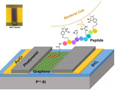
A team led by Boston College researchers has used a sheet of graphene to track the electronic signals inherent in biological structures, in order to develop a platform to selectively identify deadly strains of bacteria. This effort could lead to more accurate targeting of infections with appropriate antibiotics, according to the team.

Graphene helps create a new platform to selectively ID deadly strains of bacteria image

The prototype demonstrates the first selective, rapid, and inexpensive electrical detection of the pathogenic bacterial species Staphylococcus aureus and antibiotic resistant Acinetobacter baumannii on a single platform, said Boston College Professor of Physics Kenneth Burch, a lead co-author of the paper.

Read the full story Posted: Mar 22,2020

Navigate the emerging graphene market

This is a sponsored article by Dr Richard Collins, IDTechEx

Graphene is on the cusp of significant market growth; the opportunities are exciting and diverse, each with significant potential. Graphene and 2D Materials Europe 2020 (13-14 May, Berlin) is the largest B2B event on the topic with a dedicated focus on the commercial frontiers. www.GrapheneEurope.tech

Graphene & 2D Materials Europe 2020 leader

There is often confusion surrounding the types of graphene, commercial status, and their target markets. This article will briefly summarise each and showcase what to expect at this event.

Read the full story Posted: Feb 11,2020

Unique device that combines graphene and boron nitride can switch from superconducting to insulating

Researchers at the U.S. Department of Energy's Lawrence Berkeley National Laboratory (Berkeley Lab) have designed a graphene device that switches from a superconducting material to an insulator and back again to a superconductor — all with a flip of a switch. The team shared that the device exhibits this unique versatility while being thinner than a human hair.

Graphene and hBN device moves from insulating to superconducting imageViews of the trilayer graphene/boron nitride heterostructure device as seen through an optical microscope. The gold, nanofabricated electric contacts are shown in yellow; the silicon dioxide/silicon substrate is shown in brown and the boron nitride flakes

"Usually, when someone wants to study how electrons interact with each other in a superconducting quantum phase versus an insulating phase, they would need to look at different materials. With our system, you can study both the superconductivity phase and the insulating phase in one place," said Guorui Chen, the study's lead author and a postdoctoral researcher in the lab of Feng Wang, who led the study. Wang, a faculty scientist in Berkeley Lab's Materials Sciences Division, is also a UC Berkeley physics professor.

Read the full story Posted: Jul 18,2019

Graphene Flagship partners launch rocket to test the possibilities of printing graphene inks in space

Graphene Flagship partners, Université Libre de Bruxelles, University of Pisa and the University of Cambridge, in collaboration with the European Space Agency (ESA) and the Swedish Space Corporation (SSC), recently launched The Materials Science Experiment Rocket (MASER) into space. The objective is to test the printing of graphene patterns on silicon substrates in zero gravity conditions.

New graphene experiment launches into space image

The experiment aims to test the possibilities of printing graphene inks in space. Studying the different self-assembly modes of graphene into functional patterns in zero-gravity will enable the fabrication of graphene electronic devices during long-term space missions, as well as help understand fundamental properties of graphene printing on Earth. This mission is also a first step towards the investigation of graphene for radiation shielding purposes, an essential requirement of manned space exploration.

Read the full story Posted: Jun 25,2019

Laser technique that opens a bandgap in graphene could allow for next-gen graphene electronics

Researchers from Purdue University, the University of Michigan and the Huazhong University of Science and Technology have used a technique called "laser shock imprinting" to permanently stress graphene into having a band gap, which could mean it would be possible to use it in various electronic components.

The researchers used a laser to create shock wave impulses that penetrated an underlying sheet of graphene. The laser shock stretches the graphene onto a permanent, trench-like mold. This caused the widening of band gap in graphene to a record 2.1 electronvolts. Previously, scientists achieved 0.5 electronvolts, barely reaching the benchmark to make graphene a semiconductor like silicon.

Read the full story Posted: Jun 02,2019

Researchers bind hydrogen to graphene in a super-fast reaction that also opens up a bandgap

Researchers from Göttingen and Pasadena (USA) have produced an "atomic scale movie" showing how hydrogen atoms chemically bind to graphene in one of the fastest reactions ever studied. The team found that by adhering hydrogen atoms to graphene, a bandgap can be formed.

Hydrogen binds to graphene in 10 femtoseconds imageThe hydrogen atom (blue) hits the graphene surface (black) and forms a bond with a carbon atom (red). The high energy of the hydrogen atom is first absorbed by neighboring carbon atoms (orange and yellow) and then passed on to the graphene as a sound wave

The research team bombarded graphene with hydrogen atoms. "The hydrogen atom behaved quite differently than we expected," says Alec Wodtke, head of the Department of Dynamics at Surfaces at the Max Planck Institute (MPI) for Biophysical Chemistry and professor at the Institute of Physical Chemistry at the University of Göttingen. "Instead of immediately flying away, the hydrogen atoms 'stick' briefly to the carbon atoms and then bounce off the surface. They form a transient chemical bond," Wodtke exclaims. Something else also surprised the scientists: The hydrogen atoms have a lot of energy before they hit the graphene, but not much left when they fly away. It seems that hydrogen atoms lose most of their energy on collision, but where it goes remained to be examined.

Read the full story Posted: May 06,2019