Boron Nitride - Page 7

Versarien to supply graphene to the CPI

The advanced materials engineering group Versarien announced that it has won a tender for the ongoing supply of nanomaterials to the Centre for Process Innovation. Versarien will supply up to 1.2 kilograms of graphene in a variety of forms to the CPI, in addition to hexagonal layer boron nitride.

Neill Ricketts, chief executive of Versarien, said: "We are very pleased to have been successful in all the tenders we entered into to supply the CPI with our nanomaterials after a competitive process". "For Versarien this is an important route for the commercialization of products enhanced by graphene and other related materials", "We continue to receive record levels of enquires from potential purchasers of our products globally and look forward to making further announcements as appropriate," Ricketts said.
Read the full story Posted: Sep 19,2017

A device made from graphene and boron nitride shows unprecedented promise for spintronics applications

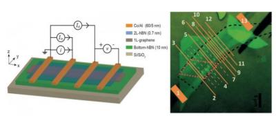
Researchers from the University of Groningen developed a device made by 2D sheets of graphene and Boron-Nitride that showed unprecedented spin transport efficiency at room temperature.

Graphene-BN device with high spin transport efficiency

The research, funded by the European Union's $1 billion Graphene Flagship, uses the single-layer graphene as the core material. The researchers say that graphene is a great material for spin transport - but the spin in the graphene cannot be manipulated. To overcome this in the device, the graphene is sandwiched between two layers of boron nitride and the whole structure rests on silicon.

Read the full story Posted: Aug 16,2017

Graphene and hBN used to develop a 2D RRAM memory device

Researchers from Soochow University in China developed a 2D RRAM device structure based on sheets of graphene and hexagonal boron nitride (hBN). The device uses a Graphene/hBN/Graphene structure and it features excellent overall fitting results.

2D Graphene / hBN RRAM design

This is still just a theoretical model, but it may prove to be the basis of high performance RRAM devices.

Read the full story Posted: Jun 01,2017

MIT team helps graphene take on exotic electronic qualities

MIT researchers have found that a flake of graphene, when brought in close proximity with two superconducting materials, can "borrow" some of those materials' superconducting qualities. When graphene is sandwiched between superconductors, its electronic state changes dramatically, even at its center.

Sandwiched between superconductors, graphene adopts exotic electronic states

The researchers showed that graphene's electrons, formerly behaving as individual particles, instead pair up in "Andreev states"—a fundamental electronic configuration that allows a conventional, non-superconducting material to carry a "supercurrent," an electric current that flows without dissipating energy.

Read the full story Posted: May 15,2017

Graphene Flagship team creates transistors printed with graphene and other layered materials

Graphene Flagship researchers from AMBER at Trinity College Dublin, in collaboration with scientists from TU Delft, Netherlands, have fabricated printed transistors consisting entirely of layered materials. The team's findings are said to have the potential to cheaply print a range of electronic devices from solar cells to LEDs and more.

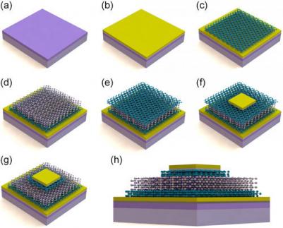
The team used standard printing techniques to combine graphene flakes as the electrodes with other layered materials, tungsten diselenide and boron nitride as the channel and separator to form an all-printed, all-layered materials, working transistor.

Read the full story Posted: Apr 09,2017

Tri-layer graphene supports a new type of magnet

A study at TIFR (Tata Institute of Fundamental Research) designed a system that allows electronic interactions to be observed in three layers of graphene. The study reveals a new kind of magnet and provides insight on how electronic devices using graphene could be made for fundamental studies as well as applications, shedding light on the magnetism of electrons in three layers of graphene at a low temperature of -272 Celsius that arises from the coordinated "whispers" between many electrons.

Metals have a large density of electrons, so being able to see the wave nature of electrons requires making metallic wires a few atoms wide. However, in graphene the density of electrons is much smaller and can be changed by making a transistor. As a result, the wave nature of electrons is easier to observe in graphene.

Read the full story Posted: Feb 26,2017

Graphene and boron nitride structure holds promise for fuel cells

Researchers at Rice University have found that layers of graphene, separated by nanotube pillars of boron nitride, may be a suitable material to store hydrogen fuel in cars. The boron nitride pillars are situated between graphene layers to make space for hydrogen atoms, similarly to spaces between floors in a building. The actual challenge is to make the atoms enter and stay in sufficient numbers and exit upon demand.

In their latest molecular dynamics simulations, the researchers found that either pillared graphene or pillared boron nitride graphene would offer abundant surface area (about 2,547 square meters per gram) with good recyclable properties under ambient conditions. Their models showed adding oxygen or lithium to the materials would make them even better at binding hydrogen.

Read the full story Posted: Oct 25,2016

Graphene Flagship team creates graphene-based quantum LEDs that emit single photons

Researchers from the Graphene Flagship have used layered materials including graphene, boron nitride and a transition metal dichalcogenide (TMD) to create all electrical quantum LEDs which can emit single photons. The devices are said to have the potential to act as on-chip photon sources in quantum information applications.

The LEDs are made of thin layers of different materials, stacked to form a heterostructure. Electrical current is injected into the device, tunnelling from single layer graphene, through a tunnel barrier of a few layers of boron nitride and into a mono- or bilayer of a transition metal dichalcogenide (TMD), such as tungsten diselenide (WSe2). In this layer, electrons recombine with holes to emit single photons.

Read the full story Posted: Sep 26,2016

Graphene enables stretchable reliable memory device for next-gen electronics

Researchers at the Korean IBS, in collaboration with Sungkyunkwan University, have designed a novel graphene-based stretchable and flexible memory device for wearable electronics.

The team has constructed a memory called two-terminal tunnelling random access memory (TRAM), where two electrodes, referred to as drain and source, resemble the two communicating neurons of the synapse in the brain. While mainstream mobile electronics use the so-called three-terminal flash memory, the advantage of two-terminal memories like TRAM is that two-terminal memories do not need a thick and rigid oxide layer. While Flash memory is more reliable and has better performance, TRAM is more flexible and can be scalable, according to the team.

Read the full story Posted: Sep 06,2016

Graphene "balloons" endure extreme pressure and could help evaluate other materials

Researchers at The University of Manchester have shown that small "balloons" made using graphene can endure huge pressures. This could be used to create miniature pressure machines that can withstand massive pressures, and pose a major step towards quickly identifying the way molecules respond under extreme pressure.

The graphene balloons normally form when depositing graphene on flat substrates and are typically thought of as a useless. The researchers at Manchester observed the nano-bubbles closely and discovered that the dimensions and shape of the nano-bubbles offer direct data regarding the elastic strength of graphene as well as its interaction with the underlying substrate. They were able to measure the pressure applied by graphene on a material caught within the balloons, or vice versa.

Read the full story Posted: Aug 26,2016