GNRs - Page 2

Researchers stabilize the edges of graphene nanoribbons and measure their magnetic properties

Researchers at Lawrence Berkeley National Laboratory (Berkeley Lab) and UC Berkeley have developed a method to stabilize the edges of graphene nanoribbons and directly measure their unique magnetic properties.

The team, co-led by Felix Fischer and Steven Louie from Berkeley Lab’s Materials Sciences Division, found that by substituting some of the carbon atoms along the ribbon’s zigzag edges with nitrogen atoms, they could discretely tune the local electronic structure without disrupting the magnetic properties. This subtle structural change further enabled the development of a scanning probe microscopy technique for measuring the material’s local magnetism at the atomic scale.

Read the full story Posted: Dec 27,2021

New method creates sub-10-nm GNRs from squashed carbon nanotubes

Researchers at Shanghai Jiao Tong University, Stanford University, and other US and China institutes have designed a strategy for creating graphene nanoribbons (GNRs) with smooth edges that are below 10 nm in width. This new method is based on the use of squashed carbon nanotubes (CNTs).

The team explained that the idea behind this new work is that if carbon nanotubes (CNTs) can be squashed into GNRs, it would be possible to produce narrow (sub-5-nm wide) GNRs from CNTs that have small diameters. The team said that the GNRs prepared using this method would be much narrower than those obtained by previous methods.

Read the full story Posted: Sep 30,2021

“Bite” defects revealed in bottom-up graphene nanoribbons

Two recent studies by a collaborative team of scientists from two NCCR MARVEL labs have identified a new type of defect as the most common source of disorder in on-surface synthesized graphene nanoribbons (GNRs).

Combining scanning probe microscopy with first-principles calculations allowed the researchers to identify the atomic structure of these so-called "bite" defects and to investigate their effect on quantum electronic transport in two different types of graphene nanoribbon. They also established guidelines for minimizing the detrimental impact of these defects on electronic transport and proposed defective zigzag-edged nanoribbons as suitable platforms for certain applications in spintronics.

Read the full story Posted: May 19,2021

Researchers design atomically precise graphene nanoribbon heterojunction sensor

An international research team, led by the University of Cologne, has succeeded in connecting several atomically precise graphene nanoribbons to form complex structures. The scientists have synthesized and spectroscopically characterized nanoribbon heterojunctions, and were able to integrate the heterojunctions into an electronic component. In this way, they have created a novel sensor that is highly sensitive to atoms and molecules.

"The graphene nanoribbon heterojunctions used to make the sensor are each seven and fourteen carbon atoms wide and about 50 nanometres long. What makes them special is that their edges are free of defects. This is why they are called "atomically precise" nanoribbons," explained Dr. Boris Senkovskiy from the Institute for Experimental Physics. The researchers connected several of these nanoribbon heterojunctions at their short ends, thus creating more complex heterostructures that act as tunneling barriers.

Read the full story Posted: May 16,2021

New method to produce graphene nanoribbons could promote use in telecommunications applications

University of WisconsinMadison researchers have fabricated graphene into the smallest ribbon structures to date, using a method that is said to make scaling-up simple. In tests with these tiny ribbons, the scientists discovered they were closing in on the properties they needed to move graphene toward usefulness in telecommunications equipment.

Flexible, easy-to-scale nanoribbons move graphene toward use in tech applications imageImage credit: University of Wisconsin−Madison

Previous research suggested that to be viable for telecommunication technologies, graphene would need to be structured prohibitively small over large areas, (which is) a fabrication nightmare, says Joel Siegel, a UWMadison graduate student in physics professor Victor Brar’s group and co-lead author of the study. In our study, we created a scalable fabrication technique to make the smallest graphene ribbon structures yet and found that with modest further reductions in ribbon width, we can start getting to telecommunications range.

Read the full story Posted: May 04,2021

Researchers design method that makes graphene nanoribbons easier to produce

Russian researchers have proposed a new method for synthesizing high-quality graphene nanoribbons. The team's approach to chemical vapor deposition offers a higher yield at a lower cost, compared with the currently used nanoribbon self-assembly on noble metal substrates.

Two nanoribbon edge configurations imageTwo nanoribbon edge configurations. The pink network of carbon atoms is a ribbon with zigzag (Z) edges, and the yellow one has so-called armchair (A) edges. Image credit MIPT

Unlike silicon, graphene does not have the ability to switch between a conductive and a nonconductive state. This defining characteristic of semiconductors is crucial for creating transistors, which are the basis for all of electronics. However, once you cut graphene into narrow ribbons, they gain semiconducting properties, provided that the edges have the right geometry and there are no structural defects. Such nanoribbons have already been used in experimental transistors with reasonably good characteristics, and the material’s elasticity means the devices can be made flexible. While it is technologically challenging to integrate 2D materials with 3D electronics, there are no fundamental reasons why nanoribbons could not replace silicon.

Read the full story Posted: Jan 12,2021

Graphene nano-ribbons could help build future integrated circuits

University of California researchers, along with teams from other U.S-based institutions like Columbia University, Lawrence Berkeley National Laboratory and University of Washington, have created a metallic wire made entirely of carbon, setting the stage for a ramp-up in research to build carbon-based transistors and, ultimately, computers.

"Staying within the same material, within the realm of carbon-based materials, is what brings this technology together now," said Felix Fischer, UC Berkeley professor of chemistry, noting that the ability to make all circuit elements from the same material makes fabrication easier. "That has been one of the key things that has been missing in the big picture of an all-carbon-based integrated circuit architecture."

Read the full story Posted: Sep 25,2020

New graphene nanoribbons could enable smaller electronic devices

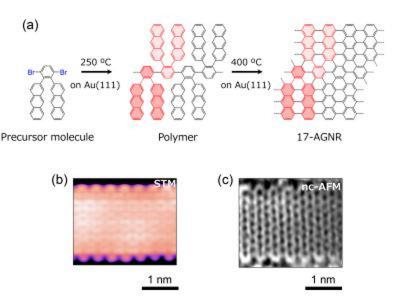
A new collaborative study has reported a 17-carbon wide graphene nanoribbon and found that it has the tiniest bandgap observed so far among familiar graphene nanoribbons prepared through a bottom-up approach.

17-carbon wide graphene nanoribbons to pave the way for new GNR-based electronic devices image(a) Bottom-up synthesis scheme of 17-AGNR on Au(111), (b) high-resolution STM image, and (c) nc-AFM image of 17-AGNR. Image Credit: Junichi Yamaguchi, Yasunobu Sugimoto, Shintaro Sato, Hiroko Yamada.

The study is part of a project of CREST, JST Japan including Nara Institute of Science and Technology (NAIST), the University of Tokyo, Fujitsu Laboratories and Fujitsu.

Read the full story Posted: Jul 06,2020

Researchers manage to grow GNRs directly on top of silicon wafers

Scientist from the University of Wisconsin-Madison are working towards making more powerful computers a reality. To that end, they have devised a method to grow tiny ribbons of graphene directly on top of silicon wafers. Graphene ribbons have a special advantage over graphene sheets - they become excellent semiconductors.

Graphene ribbons grown on silicon achieved by U of WM team imageGraphene nanoribbons on silicon wafers could help lead the way toward super fast computer chips. Image courtesy of Mike Arnold

Compared to current technology, this could enable faster, low power devices, says Vivek Saraswat, a PhD student in materials science and engineering at UW-Madison. It could help you pack in more transistors onto chips and continue Moore’s law into the future. The advance could enable graphene-based integrated circuits, with much improved performance over today’s silicon chips.

Read the full story Posted: Sep 05,2019

Graphene ribbons could enable new designs for optical quantum computers

Scientists from the University of Vienna and the Institute of Photonic Sciences in Barcelona have shown that tailored graphene structures enable single photons to interact with each other, which could lead to new designs for optical quantum computers.

Photons barely interact with the environment, making them a leading candidate for storing and transmitting quantum information. However, this feature also makes it especially difficult to manipulate information that is encoded in photons. In order to build a photonic quantum computer, one photon must change the state of a second. Such a device is called a quantum logic gate, and millions of logic gates will be needed to build a quantum computer. One way to achieve this is to use a so-called 'nonlinear material' wherein two photons interact within the material. Unfortunately, standard nonlinear materials are far too inefficient to build a quantum logic gate.

Read the full story Posted: May 07,2019