Graphene applications: what is graphene used for?
Graphene is a one-atom-thick sheet of carbon atoms arranged in a honeycomb-like pattern. Graphene is considered to be the world's thinnest, strongest and most conductive material - of both electricity and heat. All of these properties are exciting researchers and businesses around the world - as graphene has the potential to revolutionize entire industries - in the fields of electricity, conductivity, energy generation, batteries, sensors and more.
Mechanical strength
Graphene is the world's strongest material, and can be used to enhance the strength of other materials. Dozens of researchers have demonstrated that adding even a trace amount of graphene to plastics, metals or other materials can make these materials much stronger - or lighter (as you can use a smaller amount of material to achieve the same strength).

Such graphene-enhanced composite materials can find uses in aerospace, building materials, mobile devices, and many other applications.
Thermal applications
Graphene is the most heat conductive found to date. As graphene is also strong and light, it means that it is a great material for making heat-spreading solutions, such as heat sinks or heat dissipation films. This could be useful in both microelectronics (for example to make LED lighting more efficient and longer lasting) and also in larger applications - for example thermal foils for mobile devices. Huawei's latest smartphones, for example, have adopted graphene-based thermal films.

Energy storage
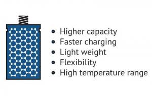
Since graphene is the world's thinnest material, it also extremely high surface-area to volume ratio. This makes graphene a very promising material for use in batteries and supercapacitors. Graphene may enable batteries and supercapacitors (and even fuel-cells) that can store more energy - and charge faster, too.
 The advantages of graphene batteries
Coatings ,sensors, electronics and more
Graphene has a lot of promise for additional applications: anti-corrosion coatings and paints, efficient and precise sensors, faster and efficient electronics, flexible displays, efficient solar panels, faster DNA sequencing, drug delivery, and more.
Graphene is such a great and basic building block that it seems that any industry can benefit from this new material. Time will tell where graphene will indeed make an impact - or whether other new materials will be more suitable.
Versarien launches new graphene biosensor chip technology
Versarien has launched a new biosensor chip utilizing novel graphene barristor sensor platform technology. These graphene barristor devices, developed in South Korea by A Barristor Company (ABC), will utilize chemical vapor deposition (CVD) grown graphene, that is produced under a Versarien license. Versarien has signed a distribution agreement with ABC to distribute the products in the UK and Europe.
A barristor (triode device) is a new type of graphene‐based transistor with a Schottky barrier between graphene and silicon. The current modulation is amplified more than 10,000 times compared to graphene field‐effect transistors (GFET), enabling the barristor transistors to overcome many GFET limitations.
Bio Graphene Solutions announces successful graphene-enhanced concrete pilot project with EllisDon Corporation in coordination with Tomlinson Ready Mix
Bio Graphene Solutions (BGS) has announced that it has completed a pilot commercial concrete pour with EllisDon Corporation, a global construction services and technology company, and Tomlinson Ready Mix, one of Ottawa’s largest concrete providers and part of the Tomlinson Group of Companies.

The Company’s proprietary graphene-enhanced admixture was integrated into the operational flow of a Tomlinson Ready Mix 32MPa-C-2 sidewalk concrete pour at an active construction project managed by EllisDon’s Ottawa team. The biographene-enhanced concrete mix utilized 10% less cement than the control mix design without sacrificing the fresh properties of the concrete. This pilot testing is a critical milestone in demonstrating the in-situ performance of the biographene-enhanced mix, validating lab trials which have shown that the concrete achieves the 28-day targeted strength of 32MPa by 7 days.
Graphene experiment proves patterns in chaos in quantum realm
Researchers from the University of California, Harvard University, University of Manchester, UC Santa Cruz and the National Institute for Materials Science in Tsukuba, Japan have conducted an experiment that confirms a 40 year old theory that electrons confined in quantum space would move along common paths rather than producing a chaotic array of trajectories.
Electrons exhibit both particle and wave-like properties and behave in ways that are often counterintuitive, and under certain conditions, their waves can interfere with each other in a way that concentrates their movement into certain patterns. Physicists call these common paths “unique closed orbits.”
Researchers use graphene in novel technique for self-assembling electronics
Researchers from North Carolina State University and Iowa State University have demonstrated a new technique for self-assembling electronic devices. The proof-of-concept work was used to create diodes and transistors, and could pave the way for self-assembling more complex electronic devices without relying on existing computer chip manufacturing techniques.
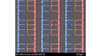
D-Met fabricated patterns produce components for potential use in microelectromechanical systems (MEMS). Image credit: Julia Chang and NCSU.
“Existing chip manufacturing techniques involve many steps and rely on extremely complex technologies, making the process costly and time consuming,” says Martin Thuo, corresponding author of a paper on the work and a professor of materials science and engineering at North Carolina State University. “Our self-assembling approach is significantly faster and less expensive. We’ve also demonstrated that we can use the process to tune the bandgap for semiconductor materials and to make the materials responsive to light – meaning this technique can be used to create optoelectronic devices. What’s more, current manufacturing techniques have low yield, meaning they produce a relatively large number of faulty chips that can’t be used. Our approach is high yield – meaning you get more consistent production of arrays and less waste.”
Graphene transistors could enable ultrasensitive detection of infections
Researchers from Friedrich Schiller University Jena, CNM Technologies, NOXXON Pharma, APTARION Biotech and Radboud University Medical Center have developed graphene field effect transistor (GFET) sensors based on van der Waals (vdW) heterostructures of single-layer graphene layered with a molecular ≈1 nm thick carbon nanomembrane (CNM).
1 / 1Schematic illustration of the fabrication steps of the l-AP/PEG-CNM GFET sensors. Credit: Advanced Materials
The CNM acts as an ultrathin molecular interposer between the graphene channel and the analyte and allows bio-functionalization without impairing the graphene properties including its charge carrier mobility.
Researchers demonstrate on-chip phonon-enhanced IR near-field detection of molecular vibrations
A team of Spain-based researchers has developed a highly sensitive detector for identifying molecules via their infrared vibrational “fingerprint”. The new detector converts incident infrared light into ultra-confined "nanolight" in the form of phonon polaritons within the detector´s active area. This mechanism serves two crucial purposes: it improves the detector's overall sensitivity and enhances the vibrational fingerprint of nanometer-thin molecular layer placed on top of the detector, allowing this molecular fingerprint to be more easily detected and analyzed.
The compact design and room-temperature operation of the device hold promise for developing ultra-compact platforms for molecular and gas sensing applications.
New method uses graphene to enable imaging of biological processes as they occur
Researchers from Radboud University Medical Center and Biointerface Laboratory RWTH Aachen University Hospital have used graphene to develop a new technique that allows them to image biological processes as they occur, with enough detail to see protein complexes move. They have demonstrated the method by showing, for the first time, how calcium deposits into a form that may lead to calcification of the arteries and aortic valve.
Schematic overview of the cryo-to-liquid-CLEM workflow. Image from: Advanced Functional Materials
The team explained that liquid phase electron microscopy (LP-EM) has emerged as a powerful technique for in situ observation of material formation in liquid. The use of graphene as window material provides, according to the scientists, new opportunities to image biological processes because of graphene's molecular thickness and electron scavenger capabilities. However, in most cases the process of interest is initiated when the graphene liquid cells (GLCs) are sealed, meaning that the process cannot be imaged at early timepoints. So, they developed a novel cryogenic/liquid phase correlative light/electron microscopy workflow that addresses the delay time between graphene encapsulation and the start of the imaging, while combining the advantages of fluorescence and electron microscopy.
New method enables materials that combine graphene and metals
Researchers from CNR-IOM, University of Milano-Bicocca, University of Trieste and University of Vienna have developed a method to create new materials that combine the extraordinary properties of single metal atoms with the robustness, flexibility, and versatility of graphene.
Co and Ni adatoms diffusing across the substrate surface before being incorporated in the growing edge of the Gr layer. Image from: Science Advances
The method involves the controlled deposition of metal atoms, such as cobalt, during the formation of the graphene layer on a nickel surface. Some of these atoms are incorporated into the carbon network of graphene, creating a material with exceptional properties of robustness, reactivity, and stability even under critical conditions.
Researchers explore the effects of physical manipulations on graphene's optical properties and conductivity
Researchers at Florida State University (FSU), Chinese Academy of Sciences (CAS) and Wuhan University have examined how physical manipulations of graphene, such as layering and twisting, impact its optical properties and conductivity.
The team, led by Assistant Professor Guangxin Ni, along with Assistant Professor Cyprian Lewandowski and graduate research assistant Ty Wilson, found that the conductivity of twisted bilayer graphene is not heavily impacted by physical or chemical manipulations and instead depends more on how the material’s minute geometry structure changes by interlayer twisting — a revelation that opens the door for additional studies on how lower temperatures and frequencies impact graphene’s properties.
HydroGraph announces breakthrough in sustainable plastic packaging research
HydroGraph Clean Power has announced a technological advancement in its sustainable plastic packaging research.

As the global polyethylene terephthalate (PET) packaging industry faces unprecedented regulatory pressure to reduce virgin plastic consumption, HydroGraph has found that its Fractal Graphene powder (FGA-1) can dramatically improve the performance and sustainability of PET bottles.
Pagination
- Page 1
- Next page


