Technical / Research

TACC signs MoU with Ceylon Graphene Technologies to advance graphene technologies

The Advanced Carbons Company (TACC), a wholly owned subsidiary of HEG, has entered into a Non-Binding Memorandum of Understanding (MOU) with Ceylon Graphene Technologies (CGT) with regard to advancing graphene technology and unlocking its vast potential for diverse applications.

CGT, a LOLC company based in Sri Lanka, is a global expert in graphene production. Leveraging Sri Lanka's premium vein graphite, renowned for its purity and backed by its expertise in material science, CGT aims to be at the forefront of delivering innovative and high-quality graphene products. TACC, part of the LNJ Bhilwara Group, is known for its expertise in synthetic graphite and commitment to sustainable, green technologies. 

Read the full story Posted: Jan 13,2025

Researchers design PV-powered supercapacitor with high energy and power density

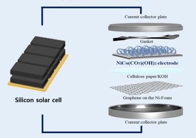
Researchers from Korea's DGIST, Kyungpook National University, France's University of Bordeaux (CNRS), Collège de France and Japan's Komaba Institute for Science (KIS) recently designed a solar-powered faradaic supercapacitor, with a graphene layer as its anode, that can reportedly achieve a power density of 2,555.6 W kg and an energy efficiency of 63%. The system uses nickel-based compounds to enhance the electrochemical performance of its electrodes.

Schematic of the system. Image from: PV Magazine, credit: Daegu Gyeongbuk Institute of Science and Technology (DGIST)

To build these electrodes, the scientists used a nickel-based carbonate and hydroxide composite material, which are said to optimize their conductivity and stability. They initially tested transition metal ions such as manganese (Mn), carbon monoxide (Co), copper (Cu), iron (Fe), and zinc (Zn) and found that the optimal nanostructure of the electrodes depended on the transition metals used.

Read the full story Posted: Jan 12,2025

New graphene-based laser lift-off process enables ultrathin flexible displays

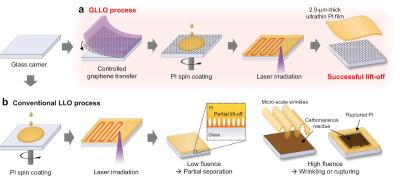
Researchers from Seoul National University of Science and Technology, Korea Advanced Institute of Science and Technology and Korea Institute of Machinery and Materials recently reported a graphene-based laser lift-off technique that prevents damage while separating ultrathin OLED displays. This advancement could open the door towards ultra-thin, stretchable devices that fit comfortably against human skin, revolutionizing wearable device technology.

a) Graphene-enabled laser lift-off (GLLO) process. b) Conventional laser lift-off (LLO) process. Image from: Nature Communications

Polyimide (PI) films are widely used in these applications due to their excellent thermal stability and mechanical flexibility. They are crucial for emerging technologies like rollable displays, wearable sensors, and implantable photonic devices. However, when the thickness of these films is reduced below 5 μm, traditional laser lift-off (LLO) techniques often fail. Mechanical deformation, wrinkling, and leftover residues frequently compromise the quality and functionality of ultrathin devices, making the process inefficient and costly.

Read the full story Posted: Jan 12,2025

Researchers develop graphene composite materials for efficient thermal management of Li-ion batteries

Researchers from China's Zhejiang University have developed a new thermal management system to prevent thermal runaway of Li-ion battery (LIB) cells, using hyperbolic graphene phase change composites. This addresses the safety concerns of LIB cells, mainly caused by thermal runaway. While phase change material systems already exist, the unresolved trade-off between high power and energy density greatly limits its practical applications. 

The newly developed thermal management system relies on a composite material that consists of hyperbolic graphene framework and paraffin, and reportedly exhibits an impressive thermal conductivity of ∼30.75 W/mK at 12.5 wt% graphene loading and ultrahigh retention (90%) of latent heat, beyond that of most of the reported phase change composites. 

Read the full story Posted: Jan 09,2025

Researchers address century-old challenge by using graphene to demonstrate diffraction of helium and hydrogen atoms

For the first time, researchers have managed to show the diffraction of atoms through a crystal. Researchers from the Institute of Quantum Technologies and the University of Vienna have demonstrated diffractions of hydrogen and helium atoms using a one-atom-thick sheet of graphene. The atoms are shot perpendicularly at the graphene sheet at high energy. While this should damage the crystal, the team succeeded in accomplishing this breakthrough without the damage.  

According to the team: "... despite decades of research, crystalline gratings used since the first atomic diffraction experiments are still unmatched regarding momentum transfer. So far, diffraction through such gratings has only been reported for subatomic particles, but never for atoms". Their recent work made use of graphene to change this situation.

Read the full story Posted: Jan 04,2025

New junction method helps control graphene's properties, could open new paths for next-gen electronics

Researchers at Korea's Pohang University of Science and Technology and Japan's National Institute for Materials Science have developed a way to control the properties of graphene by combining superconductors and graphene. 

Professor Lee Gil-ho of Pohang University of Science and Technology (POSTECH) and researchers from the Research Institute, in collaboration with Kenji Watanabe and Takashi Taniguchi from the National Institute for Materials Science (NIMS) in Japan, noted they have successfully improved the junction characteristics between graphene and superconducting electrodes. 

Read the full story Posted: Dec 31,2024

Researchers report new growth-directed graphene stacking domains that could advance next-gen electronics and quantum technologies

Graphene’ s quantum properties, such as superconductivity and other unique quantum behaviors, are known to arise when graphene atomic layers are stacked and twisted with precision to produce “ABC stacking domains.” Historically, achieving ABC stacking domains required exfoliating graphene and manually twisting and aligning layers with exact orientations—an intricate process that is difficult to scale for industrial applications.

Recently, researchers at NYU Tandon School of Engineering and Charles University in Prague, led by Elisa Riedo and Herman F. Mark, uncovered a new phenomenon in graphene research, observing growth-induced self-organized ABA and ABC stacking domains that could promote the development of advanced quantum technologies. The findings of their study demonstrate how specific stacking arrangements in three-layer epitaxial graphene systems emerge naturally — eliminating the need for complex, non-scalable techniques traditionally used in graphene twisting fabrication.

Read the full story Posted: Dec 12,2024

Graphene experiment proves patterns in chaos in quantum realm

Researchers from the University of California, Harvard University, University of Manchester, UC Santa Cruz and the National Institute for Materials Science in Tsukuba, Japan have conducted an experiment that confirms a 40 year old theory that electrons confined in quantum space would move along common paths rather than producing a chaotic array of trajectories.

Electrons exhibit both particle and wave-like properties and behave in ways that are often counterintuitive, and under certain conditions, their waves can interfere with each other in a way that concentrates their movement into certain patterns. Physicists call these common paths “unique closed orbits.”

Read the full story Posted: Dec 05,2024

Researchers use graphene in novel technique for self-assembling electronics

Researchers from North Carolina State University and Iowa State University have demonstrated a new technique for self-assembling electronic devices. The proof-of-concept work was used to create diodes and transistors, and could pave the way for self-assembling more complex electronic devices without relying on existing computer chip manufacturing techniques.

D-Met fabricated patterns produce components for potential use in microelectromechanical systems (MEMS). Image credit: Julia Chang and NCSU.

“Existing chip manufacturing techniques involve many steps and rely on extremely complex technologies, making the process costly and time consuming,” says Martin Thuo, corresponding author of a paper on the work and a professor of materials science and engineering at North Carolina State University. “Our self-assembling approach is significantly faster and less expensive. We’ve also demonstrated that we can use the process to tune the bandgap for semiconductor materials and to make the materials responsive to light – meaning this technique can be used to create optoelectronic devices. What’s more, current manufacturing techniques have low yield, meaning they produce a relatively large number of faulty chips that can’t be used. Our approach is high yield – meaning you get more consistent production of arrays and less waste.”

Read the full story Posted: Dec 04,2024

Researchers gain better understanding of electrons in pentalayer graphene

MIT researchers have gained new understanding of what leads electrons to split into fractions of themselves. Their solution sheds light on the conditions that give rise to exotic electronic states in graphene and other two-dimensional systems.

The recent work attempts to make sense of a discovery that was reported earlier this year by a different group of physicists at MIT, led by Assistant Professor Long Ju. Ju’s team found that electrons appear to exhibit “fractional charge” in pentalayer graphene — a configuration of five graphene layers that are stacked atop a similarly structured sheet of boron nitride.

Read the full story Posted: Nov 24,2024