Transistors - Page 7

Researchers produce graphene by mixing oxidized graphite with bacteria

Researchers at the U.S-based University of Rochester, along with colleagues at Delft University of Technology in the Netherlands, have designed a way to produce graphene materials using a novel technique: mixing oxidized graphite with bacteria. Their method is reportedly a more cost-efficient, time-saving, and environmentally friendly way of producing graphene materials versus those produced chemically, and could lead to the creation of innovative computer technologies and medical equipment.

Bacterially-made graphene is faster, cheaper and better imageFrom left to right:graphite (Gr), graphene oxide (GO), microbially‐reduced graphene oxide (mrGO), and chemically‐reduced graphene oxide (crGO)

"For real applications you need large amounts," says Anne S. Meyer, an associate professor of biology at the University of Rochester. "Producing these bulk amounts is challenging and typically results in graphene that is thicker and less pure. This is where our work came in". In order to produce larger quantities of graphene materials, Meyer and her colleagues started with a vial of graphite. They exfoliated the graphite-shedding the layers of material-to produce graphene oxide (GO), which they then mixed with the bacteria Shewanella. They let the beaker of bacteria and precursor materials sit overnight, during which time the bacteria reduced the GO to a graphene material.

Read the full story Posted: Jul 14,2019

Graphene biosensors detect cancer causing bacteria

Researchers at Osaka University have invented a graphene-based biosensor to detect bacteria such as those that attack the stomach lining and that have been linked to stomach cancer. When the bacteria interact with the biosensor, chemical reactions are triggered which are detected by the graphene.

Graphene-based sensors detect cancer-causing bacteria image

To enable detection of the chemical reaction products, the researchers used microfluidics to contain the bacteria in extremely tiny droplets close to the sensor surface.

Read the full story Posted: Jun 23,2019

Emberion to launch a VIS-SWIR graphene photodetector

Graphene Flagship partner, Emberion, will be launching a VIS-SWIR graphene photodetector at Laser World of Photonics, from 24 to 27 June in Munich, Germany. The linear array covers a wide spectral range, detecting wavelengths from the visible at 400nm into the shortwave infrared up to 1,800nm. Traditionally, it would require both silicon and InGaAs sensors to image across this wavelength range.

Emberion to launch a VIS-SWIR graphene photodetector image

Emberion estimates that replacing a system using silicon and InGaAs sensors with its graphene photodetector would result in a 30% cost reduction.

Read the full story Posted: Jun 19,2019

Mitsubishi develops MWIR and LWIR graphene-based sensors

Mitsubishi has reportedly developed graphene-based MWIR sensors with extraordinarily high sensitivity. Thanks to an internal graphene FET gain, the responsivity is said to be 10 times higher than that of quantum-type IR sensors with no internal amplification. Mitsubishi uses graphene FET and leverages its high electron mobility.

Mitsubishi graphene sensors image

Other than a graphene-based FET, reports suggest that there is "a light-amplifying part" that produces photoelectrons and photoholes and is placed under the graphene. At a very low temperature of, for example, 80K, the responsivity increases even more, by a factor of 100x.

Read the full story Posted: Mar 25,2019

Inorganic dopants inspire n-type graphene transistor progress

Researchers in India have made graphene field-effect transistors based on discrete inorganic structures that reportedly work for over 10 months. The approach has led them to produce a graphene logic inverter that is stable in ambient conditions.

Inorganic dopants inspire n-type graphene transistor progress image

Conventional electronics are silicon based, due to the ease of doping silicon with either electrons or holes. These two forms of silicon, n- and p-type, are the building blocks of electronic devices. However, it isn’t possible to make silicon electronics on the nanoscale, so many researchers are turning to materials like graphene.

Read the full story Posted: Mar 14,2019

Paragraf starts producing graphene at commercial scale

University of Cambridge spin-out company, Paragraf, recently announced that it started producing graphene at up to eight inches (20cm) in diameter, large enough for commercial electronic devices.

Paragraf is producing graphene ‘wafers’ and graphene-based electronic devices, which could be used in transistors, where graphene-based chips could deliver speeds more than ten times faster than silicon chips; and in chemical and electrical sensors, where graphene could increase sensitivity by a factor of more than 30. The company’s first device will reportedly be available in the next few months.

Read the full story Posted: Mar 14,2019

Graphene quantum dots to help create single electron transistors

Scientists from Manchester University, the Ulsan National Institute of Science & Technology and the Korea Institute of Science and Technology have developed a novel technology, which combines the fabrication procedures of planar and vertical heterostructures in order to assemble graphene-based single-electron transistors.

Graphene quantum dots to help create single electron transistorsThe schematic structure of the devices

In the study, it was demonstrated that high-quality graphene quantum dots (GQDs), regardless of whether they were ordered or randomly distributed, could be successfully synthesized in a matrix of monolayer hexagonal boron nitride (hBN). Here, the growth of GQDs within the layer of hBN was shown to be catalytically supported by the platinum (Pt) nanoparticles distributed in-between the hBN and supporting oxidised silicon (SiO2) wafer, when the whole structure was treated by the heat in the methane gas (CH4). It was also shown, that due to the same lattice structure (hexagonal) and small lattice mismatch (~1.5%) of graphene and hBN, graphene islands grow in the hBN with passivated edge states, thereby giving rise to the formation of defect-less quantum dots embedded in the hBN monolayer.

Read the full story Posted: Mar 08,2019

Korean researchers fabricate ordered graphene quantum dot arrays

A new study led by the Ulsan National Institute of Science and Technology in South Korea reveals a technology capable of fabricating highly ordered arrays of graphene quantum dots.

Korean researchers fabricate ordered graphene quantum dot arrays imageGraphene quantum dots of various sizes in a stable, ordered array

The research team demonstrated a novel way of synthesizing GQDs, embedded inside a hexagonal boron nitride (hBN) matrix. Thus, they demonstrated simultaneous use of in-plane and van der Waals heterostructures to build vertical single-electron tunneling transistors.

Read the full story Posted: Feb 10,2019

Italian researchers develop a graphene-based OFET for future OLED and OLET displays

Researchers from Italy's ISOF-CNR, University of Naples "Federico II" and Università di Modena e Reggio Emilia have developed new organic n-type FET transistors (OFETs) based on CVD graphene sheets. The researchers say that the new process and materials they used can enable flexible, transparent and short-channel OFETs - which could be used in the future for OLED or OLET (organic light emitting transistor) displays.

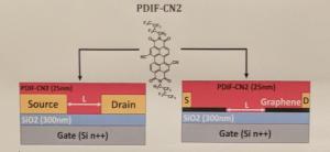
ISOF CNF CVD graphene OFET structure photo

To create the new transistors, the researchers used thermally evaporated thin-films of PDIF-CN2 (a perylene diimide derivative) as the the organic semiconductor for the active channel of the transistor with the single-layer CVD graphene (grown at Italy's IIT institute) as the electrode material. The final device architectures have been fabricated via Electron-Beam-Lithography (EBL) and Reactive Ion Etching (RIE).

Read the full story Posted: Jan 28,2019

Graphenea GFAB: Graphene Foundry Service Launched

This is a sponsored post by Graphenea

Graphenea recently launched a graphene foundry service GFAB. The company will manufacture custom circuit designs on graphene wafers up to 6. The service is aimed at enabling fast device prototyping and accelerating development of new applications, lowering entry barriers to graphene-based solutions.

Graphenea states that in view of the market demands, the offer now includes small batch sizes (1-3 wafers). Lithography masks can be manufactured by Graphenea or provided by the customer. GFAB includes graphene growth, transfer on 4 and 6 wafers, metal contact deposition and lift-off, and graphene lithography with etching.

Read the full story Posted: Jan 22,2019