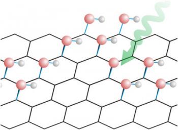
Researchers from Technological Center AIMEN explored the use of ultrafast lasers as tools for graphene processing and found that laser beams can be focused to tailor the properties of graphene films in finely defined areas to produce distinct behaviors useful for various devices. The speed of the process can be higher than one m/s for drawing the micrometer-sized features. Processing speeds over 10 m/s could be attained using advanced optical scanning.

The method is based on the use of short, highly controlled laser pulses, which induce chemical changes in the carbon lattice. A single pulse of laser with a duration of several picoseconds is enough. At this timescale, the researchers demonstrated that they can pattern graphene lattices by cutting, adding external molecules or binding compounds (functional groups like oxygen or hydroxyl). As the laser spot can be focused in an area of one square micron or less, direct writing of devices on graphene can be achieved with high precision, producing nano-devices with minimal footprint and maximum efficiency.
In addition to demonstrating laser-based, large-scale patterning of graphene at high speed and resolution, the researchers also showed the control of the thermal and chemical processes by adjusting laser beam characteristics. For low energy inputs, multiphoton absorption plays a major role, inducing chemical reactions between carbon and atmosphere molecules, resulting in new optical properties in graphene. This research lays a foundation for deeper understanding of the chemical and physical processes for industrially feasible graphene patterning, as well as tests for real device applications for future electronics.