The exceptional electronic properties of graphene make it a material with large potential for low-power, high-frequency electronics. However, the performance of a graphene-based device depends not only on the properties of the graphene itself, but also on the quality of its metal contacts. The lack of effective and manufacturable approaches to establish good ohmic contacts to a graphene sheet is one of the factors that currently limit the full application potential of graphene technology. The quality of the graphene-metal contacts is described in terms of the contact resistance (RC). Low RC values are crucial for any high-frequency or low-power application. Graphene’s low density of states near the charge neutrality point (Dirac point) limits carrier injection from metals, often resulting in high RC values.
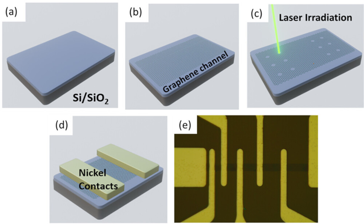
(a–d) Schematics showing the process sequence for manufacturing the devices and the laser irradiation of graphene in the contact regions. (e) Optical micrograph of one of the measured devices. Image credit: AMO
Recently, researchers from RWTH Aachen University and AMO have developed a scalable method based on laser irradiation of graphene to reduce the RC in nickel-contacted devices. A laser with a wavelength of l = 532 nm is used to induce defects at the contact regions, which are monitored in situ using micro-Raman spectroscopy.
Physical damage is observed using ex situ atomic force and scanning electron microscopy. The transfer length method (TLM) is used to extract RC from back-gated graphene devices with and without laser treatment under ambient and vacuum conditions.
A significant reduction in RC was observed in devices where the contacts were laser irradiated, which scales with the laser power. The lowest RC of about 250 Ω μm was obtained for the devices irradiated with a laser power of 20 mW, compared to 900 Ω μm for the untreated devices.
The reduction is attributed to an increase in defect density, which leads to the formation of crystallite edges and in-plane dangling bonds that enhance the injection of charge carriers from the metal into the graphene.
The proposed method can be easily scaled, implemented, and automated to engineer the RC in graphene and potentially other 2D material-based devices.