Boron Nitride - Page 2

Researchers use graphene to design transformable nano-scale electronic devices

Researchers at University of California, Irvine, working with a team from Japan's National Institute for Materials Science, have reported the discovery of nano-scale devices that can transform into many different shapes and sizes even though they exist in solid states. This comes in contrast to conventional nano-scale electronic parts in devices like smartphones, that are solid, static objects that once designed and built cannot transform into anything else. This recent finding could fundamentally change the nature of electronic devices, as well as the way scientists research atomic-scale quantum materials. 

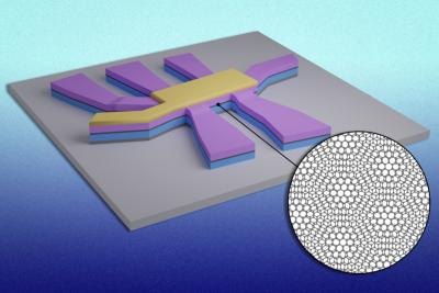
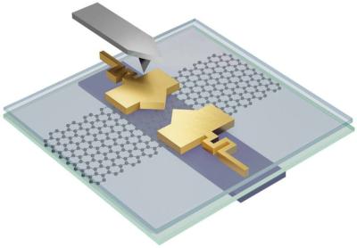
 Schematic of an hBN-encapsulated graphene device with a local graphite back gate and flexible serpentine leads connected to the movable QPC top gates (metal contacts to the graphene and graphite not shown). Image from Science Advances

“What we discovered is that for a particular set of materials, you can make nano-scale electronic devices that aren’t stuck together,” said Javier Sanchez-Yamagishi, an assistant professor of physics & astronomy whose lab performed the new research. “The parts can move, and so that allows us to modify the size and shape of a device after it’s been made.”
Read the full story Posted: Apr 19,2023

Graphene quantum dots could improve magnetic field sensors

Researchers from the University of California Santa Cruz, University of Manchester and Japan's International Center for Materials Nanoarchitectonics and National Institute for Materials Science have used a scanning tunnelling microscope to create and probe single and coupled electrostatically defined graphene quantum dots, to investigate the magnetic-field responses of artificial relativistic nanostructures.

Trapped electrons traveling in circular loops at extreme speeds inside graphene quantum dots are highly sensitive to external magnetic fields and could be used as novel magnetic field sensors with unique capabilities. Although graphene electrons do not move at the speed of light, they exhibit the same energy-momentum relationship as photons and can be described as "ultra-relativistic." When these electrons are confined in a quantum dot, they travel at high velocity in circular loops around the edge of the dot.

Read the full story Posted: Mar 07,2023

Graphene used to grow the world's smallest microLEDs and highest-density microLED arrays

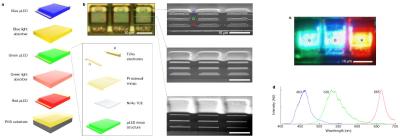
Researchers from MIT, in collaboration with researchers from other Universities in the US and Korea, have used graphene (and hBN) to develop full-color vertically-stacked microLEDs  - that achieve the highest array density (5100 PPI) and the smallest size (4 µm) reported to date.

The researchers developed a 2D-materials based layer transfer (2DLT) technique - that involves growing the LEDs on 2D material-coated substrates, removing the LEDs, and then sttacking them. For the red LEDs, the researchers used graphene, coated on a GaAs wafer, while for the green and blue LEDs, they used hBN on sapphire wafers. The graphene red LEDs were transferred using remote epitaxy, while the hBN blue and green ones were removed using Van der Waals epitaxy.

Read the full story Posted: Feb 02,2023

Researchers find superconductivity that can be turned on and off in "magic angle" graphene

Researchers at MIT and National Institute for Materials Science in Tsukuba, Japan, have found a new and intriguing property of “magic-angle” graphene: superconductivity that can be turned on and off with an electric pulse, much like a light switch.

The discovery could lead to ultrafast, energy-efficient superconducting transistors for neuromorphic devices — electronics designed to operate in a way similar to the rapid on/off firing of neurons in the human brain.

Read the full story Posted: Jan 29,2023

PlanarTECH on its way to its best year ever, gets ready for its second crowdfunding round

UK-based PlanarTECH offers R&D and production-scale equipment and services for all classes of emerging 2D materials and carbon-based materials such as CNTs and CVD diamonds. In 2020 planarTECH launched a successful equity crowdfunding campaign as it aims to expand its business and enter new markets such as industrial CVD graphene production systems and material production.

We have recently talked to the company's CEO, J. Patrick Frantz, who gives us the latest business and technology updates from PlanarTECH.

Q: Can you update us on your latest business activities, with a focus on graphene?

We had a very difficult time during the pandemic, as many companies did. From July 2020 through June 2021 we shipped just one CVD system. However, we started to see a resumption of customer activity towards the end of 2021 as labs reopened and people around the world got back to work. For 2022, we’re seeing a complete recovery and are on our way to the best year we’ve ever had in terms of sales.

Read the full story Posted: Dec 07,2022

Various graphene technologies to be tested during moon and space missions

Graphene Flagship Partners University of Cambridge (UK) and Université Libre de Bruxelles (ULB, Belgium) collaborated with the Mohammed bin Rashid Space Centre (MBRSC, United Arab Emirates) and the European Space Agency (ESA) to test graphene on the Moon. This joint effort sees the involvement of many international partners, such as Airbus Defense and Space, Khalifa University, Massachusetts Institute of Technology, Technische Universität Dortmund, University of Oslo, and Tohoku University.

The MASER15 launch. Credit: John-Charles Dupin/Eurekalert

The Rashid rover is planned to be launched today (30 November 2022) from Cape Canaveral in Florida and will land on a geologically rich and, as yet, only remotely explored area on the Moon’s nearside – the side that always faces the Earth. During one lunar day, equivalent to approximately 14 days on Earth, Rashid will move on the lunar surface investigating interesting geological features.

Read the full story Posted: Nov 30,2022

Researchers show that hydrodynamic electrons flow through materials without electrical resistance

Scientists from Israel's Weizmann Institute of Science, in collaboration with teams at Manchester University and UC Irvine,  have shown that an electronic fluid can flow through materials without any electrical resistance, thereby perfectly eliminating a fundamental source of resistance that forms the ultimate limit for ballistic electrons. This result could open the door to improved electronic devices that do not heat up as much as existing technologies.

When electrons flow in electrical wires, they lose part of their energy, which is wasted as heat. This heating is a major problem in everyday electronics. The heating occurs because electrical conductors are never perfect and have a resistance for the flow of electrical currents. Typically, this resistance originates from the scattering of the flowing electrons by imperfections in the host material. But it stands to reason that a perfect conductor, devoid of any imperfections, would have zero resistance. However, even if the conductor is perfectly clean and free from imperfections, the resistance does not vanish. Instead, a new source of resistance emerges, known as the Landauer-Sharvin resistance. In an electrical conductor, electrons flow in quantum channels, much like cars in highway lanes. Similar to highway lanes, each electronic channel has a finite capacity to conduct electrons, limited by the quantum of conductance. For a given conductor, the number of quantum channels is finite and determined by its physical width. Thus, even a perfect electronic device, devoid of any imperfections, will never have infinite conductance. It will always have resistance. In the absence of interactions between electrons, this Landauer-Sharvin resistance is unavoidable, putting a fundamental lower bound on the heating of computer chips, which becomes even more severe as transistors become smaller.

Read the full story Posted: Sep 14,2022

Researchers develop graphene-based foam composite for efficient water filtration

While graphene-based materials have potential as adsorbent materials, their performance can be hindered due to aggregation and a lack of control over their porosities and dimensions. The researchers in a recent study, from the University of Exeter, Kyushu University and the University of Oxford, have addressed this issue by developing a unique graphene material combined with a high porosity composite foam to combat aggregation.

Pharmaceuticals are among the most prominent emerging contaminants (ECs) in water systems. They may cause severe environmental consequences along with potential health problems. To successfully eradicate ECs from processed wastewater streams, effluent and drinking water purification facilities must adopt adequate tertiary treatment methods. Adsorption is regarded as a technology with great potential in water treatment as it is dependable and less expensive compared to reverse osmosis, oxidizing, microfiltration, ultrafiltration, ion exchange, etc.

Read the full story Posted: Jun 07,2022

Researchers succeed in synthesizing single layers of hexagonal boron nitride on graphene

A research team led by the University of Michigan has developed a reliable, scalable method for growing single layers of hexagonal boron nitride on graphene.

Graphene-hBN structures can power LEDs that generate deep-UV light, which is impossible in today's LEDs, said Zetian Mi, U-M professor of electrical engineering and computer science and a corresponding author of the study. Deep-UV LEDs could drive smaller size and greater efficiency in a variety of devices including lasers and air purifiers.

Read the full story Posted: Apr 24,2022

Researchers detect evidence of strong electron correlation in a trilayer graphene/hBN moiré superlattice

Researchers from MIT, Harvard University, University of California at Berkeley, Lawrence Berkeley National Laboratory, China's Shanghai Jiao Tong and Fudan Universities and Japan's National Institute for Materials Science have taken a significant step toward understanding electron correlations.

In their new study, the researchers revealed direct evidence of electron correlations in a two-dimensional material called ABC trilayer graphene. This material has previously been shown to switch from a metal to an insulator to a superconductor.

Read the full story Posted: Mar 22,2022