Boron Nitride - Page 3

Redmi K50 e-sports version sports an advanced graphene-based cooling system

Graphene-based cooling systems are becoming quite popular in today's cellphones, with many companies using it in their models. A few examples are: realme's GT 2 series, ZTE's Axon 30, Xiaomi's Mi 10 Ultra, various Huawei phones and more.

REDMI K50 E-SPORTS uses graphene cooling systems image

Now, it seems that Redmi's K50 e-sports has joined this team, with a recent disassembly test that found that its heat dissipation system makes use of graphene films. The test also reported 3D high-power graphite, large-area double VC, and heat dissipation copper sheet + boron nitride.

Read the full story Posted: Feb 22,2022

Graphene and hBN nano-additives improve eco-friendly lubricant oils

Researchers from the University of Nevada have investigated the introduction of graphene nanoplatelets (GNPs) and hexagonal boron nitride (hBN) to canola oil to improve its tribological properties, as part of an effort to reduce the usage of lubricants based on petroleum as lubricants for reducing abrasion and friction.

Three nanoscale lubricating combinations were created by combining both GNP and hBN settings in varied ratios to get the best beneficial synergy. The team reports that lubrication quality and performance may be increased by using low-weight percentages of nanoparticle (NP) and microparticle additions. One benefit is that it has a reduced coefficient of friction (COF) and wearing.

Read the full story Posted: Jan 05,2022

Boron nitride assists in protecting graphene in order to achieve next-gen electronics

Researchers from AMO, Oxford Instruments, Cambridge University, RWTH Aachen University and the University of Wuppertal have demonstrated a new method to use plasma enhanced atomic layer deposition (PEALD) on graphene without introducing defects into the graphene itself.

Currently, the most advanced technique for depositing dielectrics on graphene is atomic layer deposition (ALD), which allows to precisely control the uniformity, the composition and the thickness of the film. The process typically used on graphene and other 2D materials is thermal water-based ALD, as it does not damage the graphene sheet. However, the lack of nucleation sites on graphene limits the quality of the dielectric film, and requires the deposition of a seed layer prior to ALD to achieve good results. Another approach is plasma enhanced atomic layer deposition (PEALD), which, when applied to growth on graphene, can introduce surface damage. This is what to team addressed in this recent work.

Read the full story Posted: Aug 09,2021

Researchers show that stretching can change the electronic properties of graphene

A research team led by the University of Basel has found that the electronic properties of graphene can be specifically modified by stretching the material evenly.

The researchers, led by Professor Christian Schönenberger at the Swiss Nanoscience Institute and the Department of Physics at the University of Basel, have studied how the material’s electronic properties can be manipulated by mechanical stretching. In order to do this, they developed a kind of rack by which they stretch the atomically thin graphene layer in a controlled manner, while measuring its electronic properties.

Read the full story Posted: Jun 29,2021

Researchers report a highly efficient graphene/hBN-based electro-absorption modulator

ICFO researchers led by Professor Frank Koppens, in collaboration with researchers from Universita di Pisa, CNIT, Ghent University-IMEC, and NIMS, have reported a novel electro-absorption (EA) modulator capable of showing a 3-fold increase in static and dynamic modulation efficiency while maintaining the high-speed, a value that surpasses those for previously reported graphene EA modulators.

 Electrical connections and schematic cross-section of an EA modulator with an hBNHfO2hBN dielectric image

To achieve this, the team of researchers developed a high-quality graphene-based electro-absorption modulator by combining high-quality graphene and a high-k dielectric, also used in microelectronics. The high quality of the graphene was achieved by integrating it with the 2d-material dielectric hexagonal boron nitride (hBN).

Read the full story Posted: Feb 16,2021

Scientists discover important new property of graphene

MIT researchers and colleagues have discovered a new and important electronic property of graphene. The work, which involves structures composed of atomically thin layers of materials that are also biocompatible, could usher in new, faster information-processing paradigms. One potential application is in neuromorphic computing, which aims to replicate the neuronal cells in the body responsible for everything from behavior to memories.

Graphene-based heterostructures continue to produce fascinating surprises. Our observation of unconventional ferroelectricity in this simple and ultra-thin system challenges many of the prevailing assumptions about ferroelectric systems and it may pave the way for an entire generation of new ferroelectrics materials, says Pablo Jarillo-Herrero, the Cecil and Ida Green Professor of Physics at MIT and leader of the work, which involved a collaboration with five other MIT faculty from three departments.

Read the full story Posted: Jan 27,2021

AIXTRON's new graphene and hBN industrial grade reactor goes into operation

AIXTRON has developed, built and installed a new, specific industrial grade reactor for graphene and hexagonal Boron Nitride (hBN) processing on 200 mm epi-wafers. The new CVD tool was developed as part of the GIMMIK research project and has recently gone into operation.

The GIMMIK project aims to evaluate the production of graphene layers under industrial conditions, spotting weak points and designing ways of eliminating the sources of error. Furthermore, the transfer of the properties of graphene to electrical components by integration into a material environment are to be tested. In parallel, methods for the large-area, contact-free characterization of graphene will be developed, which do not yet exist at present. The GIMMIK research project aims to expand graphene technology for electronic components and to bring it up to a production-relevant level. Participants of the GIMMIK project include: AIXTRON SE, Infineon Technologies, IHP GmbH - Leibniz-Institut für innovative Mikroelektronik, Protemics, LayTec, RWTH Aachen.

Read the full story Posted: Dec 22,2020

Researchers achieve direct visualization of of quantum dots in bilayer graphene

Researchers at UC Santa Cruz have reported the first direct visualization of quantum dots in bilayer graphene, revealing the shape of the quantum wave function of the trapped electrons. The finding of this research could provide important fundamental knowledge, required for developing quantum information technologies based on bilayer graphene quantum dots.

Direct visualization of quantum dots reveals shape of quantum wave function imageImage from Nano Letters

"There has been a lot of work to develop this system for quantum information science, but we've been missing an understanding of what the electrons look like in these quantum dots," said corresponding author Jairo Velasco Jr., assistant professor of physics at UC Santa Cruz.

Read the full story Posted: Nov 25,2020

University of Manchester team discovers a new family of quasiparticles in graphene-based superlattices

Researchers at The University of Manchester, led by Sir Andre Geim and Dr Alexey Berdyugin, have discovered and characterized a new family of quasiparticles named 'Brown-Zak fermions' in graphene-based superlattices. This was achieved by aligning the atomic lattice of a graphene layer to that of an insulating boron nitride sheet, dramatically changing the properties of the graphene sheet.

The study follows years of successive advances in graphene-boron nitride superlattices which has previously allowed the observation of a fractal pattern known as the Hofstadter's butterfly - and now, with this current work, the researchers report another highly surprising behavior of particles in such structures under applied magnetic field.

Read the full story Posted: Nov 14,2020

Researchers examine novel inkjet-printed graphene for high‐quality large‐area electronics

Researchers from the University of Nottingham’s Centre for Additive Manufacturing (CfAM) have reported a breakthrough in the study of 3D printing electronic devices with graphene.

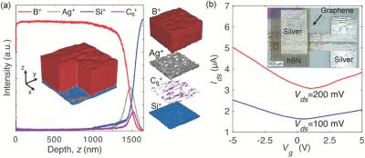
inkjet‐printed graphene/hBN FET imageCharacterization of the fully inkjet‐printed graphene/hBN FET. Photo from article

The scientists utilized an inkjet-based 3D printing technique to deposit inks that contained flakes of graphene, in a promising step towards replacing single-layer graphene as a contact material for 2D metal semiconductors.

Read the full story Posted: Nov 09,2020