Electronics - Page 16

Graphene enables color changing electronic skin

Researchers from Tsinghua University in China have developed a graphene-based user-interactive electronic skin, capable of changing color. The team made use of flexible electronics made from graphene, in the form of a highly-sensitive resistive strain sensor, combined with a stretchable organic electrochromic device.

To obtain good performance with a simple process and reduced cost, they designed a structure to use graphene as both the highly sensitive strain-sensing element and the insensitive stretchable electrode of the electric current density (ECD) layer.

Read the full story Posted: Jul 31,2017

Researchers demonstrate a chemical pathway to using graphene in electronics

Researchers from Utrecht University, TU Delft and the Aalto University in Finland have shown that electronic components can be incorporated in single graphene wires (nanoribbons) with atomic precision. The result is a working electronic device that could be used in graphene-based electronic switches with extremely fast operational speeds.

Chemical route to graphene electronics image

The researchers state that their solution to using graphene in electronics is atomically precise; By selecting certain precursor substances (molecules), the team can code the structure of the electrical circuit with extreme accuracy. The switch is based on the principle of graphene nanoribbons. Previous research has shown that the ribbon’s electronic characteristics are dependent on its atomic width. A ribbon that is five atoms wide is an ordinary electric wire with extremely good conduction characteristics, but adding two atoms makes the ribbon a semiconductor. We are now able to seamlessly integrate a five-atom wide ribbon together with one that is seven atoms wide. That gives you a metal-semiconductor junction, which works as a diode, according to the team.

Read the full story Posted: Jul 27,2017

Chinese team created graphene aerogels inspired by plant structure

Researchers at Zhejiang University in China have designed a graphene-based aerogel mimicking the structure of the "powdery alligator-flag" plant that could have potential for use in applications like flexible electronics.

Graphene aerogel based on plant structure image

The team drew inspiration from the stem structure of the powdery alligator-flag plant (Thalia dealbata), a strong, lean plant capable of withstanding harsh winds. The researchers used a bidirectional freezing technique that they previously developed to assemble a new type of biomimetic graphene aerogel that had an architecture like that of the plant's stem. When tested, the material supported 6,000 times its own weight and maintained its strength after intensive compression trials and was resilient. They also put the aerogel in a circuit with a LED and found it could potentially work as a component of a flexible device.

Read the full story Posted: Jun 22,2017

Graphene electrodes may open new paths in molecular electronic devices

An international team of researchers, led by the University of Bern and the National Physical Laboratory (NPL) and assisted by the University of the Basque Country (UPV/EHU, Spain) and Chuo University (Japan), has demonstrated a new way to control the functionality of next-gen molecular electronic devices using graphene. The results could be used to develop smaller, higher-performance devices for use in a applications like sensors, flexible electronics, energy conversion and storage, and more.

The team demonstrated the stability of multi-layer graphene-based molecular electronic devices down to the single molecule limit. The findings represent a major step change in the development of graphene-based molecular electronics, with the reproducible properties of covalent contacts between molecules and graphene (even at room temperature) reportedly overcoming the limitations of current state-of-the-art technologies based on coinage metals.

Read the full story Posted: Jun 12,2017

High performance graphene transistors developed by Graphene Flagship researchers

An international team of scientists collaborating in the Graphene Flagship project has developed a graphene-based transistor that reportedly outperforms previous state-of-the-art ones. The team utilized a thin top gate insulator material to optimize operational properties like maximum oscillation frequency, cutoff frequency, forward transmission coefficient, and open-circuit voltage gain, realizing devices that show prospect of using graphene in a wide range of electronic applications.

Graphene Flagship team develops high performance graphene transistors image

Graphene lack of a bandgap hinders its use in electronics since it causes an inability to switch the transistors off, effectively rendering the 0 state in digital logic inaccessible. However, many analog applications do not require a bandgap; The team explains that the only undesired side-effect of using GFETs in analog circuits is a poor saturation of the drain current, which prevents high-gain operation. The researchers have now succeeded in improving saturation by optimizing the dielectric material (AlOx) that is used to electrically insulate the top gate of the GFET. An improved quality of gate dielectric resulted in strong control over carriers in the graphene channel, yielding overall performance benefits.

Read the full story Posted: Jun 07,2017

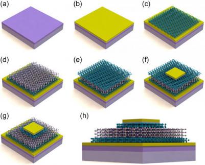
Graphene and hBN used to develop a 2D RRAM memory device

Researchers from Soochow University in China developed a 2D RRAM device structure based on sheets of graphene and hexagonal boron nitride (hBN). The device uses a Graphene/hBN/Graphene structure and it features excellent overall fitting results.

2D Graphene / hBN RRAM design

This is still just a theoretical model, but it may prove to be the basis of high performance RRAM devices.

Read the full story Posted: Jun 01,2017

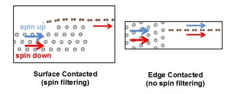
Manipulating the electron spin can lower the contact resistance in graphene-metal interfaces

NUS researchers discovered that manipulating the electron spin lowers the contact resistance in graphene-metal interfaces, which normally suffer from large electrical resistance.

Spin filtering in metal-graphene interfaces image

The researchers have shown that edga-contacted device geometries in metallic-graphene interfaces feature some of the lowest contact resistances reported to date - significantly lower than in surface-contracted interfaces. The researchers explain that this is due to the different behavior of electron spins in these geometries.

Read the full story Posted: May 22,2017

Graphenea and U of Hamburg team upscale high-quality graphene devices

Researchers from the University of Hamburg and Graphenea have succeeded in upscaling high-quality graphene devices to the 100-micron scale and beyond. By perfecting CVD graphene production, transfer and patterning processes, the team managed to observe the quantum Hall effect in devices longer than 100 micrometers, with electronic properties on par with micromechanically exfoliated devices.

Graphenea upscales graphene devices

The work started from graphene grown by chemical vapor deposition (CVD) on a copper substrate. Since graphene on metal is not useful for applications in electronics, the material is usually transferred onto another substrate before use. The transfer process has proven to be a challenge, in many cases leading to cracks, defects, and chemical impurities that reduce the quality of the graphene.

Read the full story Posted: May 07,2017

Graphene-based contact lens sensor for diabetes monitoring

Researchers affiliated with UNIST have raised the possibility of in-situ human health monitoring by wearing a contact lens with built-in wireless smart sensors. Towards this end, the team made use of smart contact lens sensors with electrodes made of graphene sheets and metal nanowires.

Graphene lens sensor for disease monitoring image

The smart contact lens sensor could help monitor biomarkers for intraocular pressure (IOP), diabetes mellitus, and other health conditions. The research team expects that this research breakthrough could lead to the development of biosensors capable of detecting and treating various human diseases, and used as a component of next-generation smart contact lens-related electronic devices.

Read the full story Posted: May 03,2017

Researchers succeed in imaging how electrons move in graphene

Researchers at the University of Melbourne succeeded in imaging how electrons move in 2D graphene, an achievement which may boost the development of next-generation electronics. The new technique overcomes usual limitations of existing methods for understanding electric currents in devices based on ultra-thin materials, and so it is capable of imaging the behavior of moving electrons in structures only one atom in thickness.

Mapping electrons in graphene using diamonds image

The team used a special quantum probe based on an atomic-sized 'color center' found only in diamonds to image the flow of electric currents in graphene. The technique could be used to understand electron behavior in a variety of new technologies.

Read the full story Posted: Apr 27,2017