MIT - Page 3

Researchers create tunable superconductivity in magic-angle twisted trilayer graphene

When two sheets of graphene are stacked atop each other at just the right angle, the layered structure morphs into an unconventional superconductor, allowing electric currents to pass through without resistance or wasted energy. This magic-angle transformation in bilayer graphene was observed for the first time in 2018 in the group of Pablo Jarillo-Herrero at MIT. Since then, scientists have searched for other materials that can be similarly twisted into superconductivity, but for the most part, no other twisted material has exhibited superconductivity other than the original twisted bilayer graphene.

Stacking order imageIllustrations of A-tw-A stacking (a) and A-tw-B stacking (b). Image from Nature

In a recent paper, Jarillo-Herrero and his group reported observing superconductivity in a sandwich of three graphene sheets, the middle layer of which is twisted at a new angle with respect to the outer layers. This new trilayer configuration reportedly exhibits superconductivity that is more robust than its bilayer counterpart.

Read the full story Posted: Feb 02,2021 - 1 comment

Scientists discover important new property of graphene

MIT researchers and colleagues have discovered a new and important electronic property of graphene. The work, which involves structures composed of atomically thin layers of materials that are also biocompatible, could usher in new, faster information-processing paradigms. One potential application is in neuromorphic computing, which aims to replicate the neuronal cells in the body responsible for everything from behavior to memories.

Graphene-based heterostructures continue to produce fascinating surprises. Our observation of unconventional ferroelectricity in this simple and ultra-thin system challenges many of the prevailing assumptions about ferroelectric systems and it may pave the way for an entire generation of new ferroelectrics materials, says Pablo Jarillo-Herrero, the Cecil and Ida Green Professor of Physics at MIT and leader of the work, which involved a collaboration with five other MIT faculty from three departments.

Read the full story Posted: Jan 27,2021

International team develops ultrasensitive graphene-based microwave detector

A joint international research team, including teams from POSTECH of South Korea, Raytheon BBN Technologies, Harvard University, and Massachusetts Institute of Technology in the U.S., Barcelona Institute of Science and Technology in Spain, and the National Institute for Materials Science in Japan, has developed ultrasensitive sensors that can detect microwaves with the highest theoretically possible sensitivity. The research findings are drawing attention as an enabling technology for commercializing next-gen technologies like quantum computers.

Graphene-based Josephson junction microwave bolometer imageMicrowave bolometer based on graphene josephson junction. Image credit: Raytheon BBN Technologies and MIT

Microwave is used in a wide range of scientific and technological fields, including mobile communications, radar, and astronomy. Currently, microwave power can be detected using a device called bolometer. A bolometer usually consists of three materials: Electromagnetic absorption material, a material that converts electromagnetic waves into heat, and a material that converts the generated heat into electrical resistance. The bolometer calculates the amount of electromagnetic waves absorbed using the changes in the electrical resistance. Using the semiconductor-based diodes such as silicon and gallium arsenide in the bolometer, the sensitivity of the state-of-the-art commercial bolometer operating at room temperature is limited at 1 nanowatt (1 billionth of a watt) by averaging for a second.

Read the full story Posted: Oct 03,2020

MIT team reports new roll-to-roll process for production of large sheets of high-quality graphene

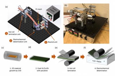
Researchers at MIT have developed a new roll-to-roll production process for large sheets of high-quality graphene, which the team says could lead to ultra-lightweight, flexible solar cells, and to new classes of light-emitting devices and other thin-film electronics.

MIT develops roll-to-roll process for graphene production image

The new manufacturing process, which the team says should be relatively easy to scale up for industrial production, involves an intermediate buffer layer of material that is key to the technique’s success. The buffer allows the ultrathin graphene sheet, less than a nanometer (billionth of a meter) thick, to be easily lifted off from its substrate, allowing for rapid roll-to-roll manufacturing.

Read the full story Posted: Jun 09,2020

MIT team finds ‘twisted’ graphene getting weirder at ‘magical angle’

Researchers at the Massachusetts Institute of Technology (MIT) have previously found a particularly strange pattern in the twisted graphene structure, and now they’ve studied it more closely and found that the more layers it has, the better it will work.

Graphene is a 2D carbon nanomaterial consisting of a hexagonal hexagonal grid of a hexagonal structure of carbon atoms with a sp2 hybrid orbit. This makes them functionally two-dimensional, because the electrons that move through them can only move forward/backward and sideways, not above and below. This makes graphene very conductive.

Read the full story Posted: May 12,2020

MIT researchers use graphene and boron nitride to convert terahertz waves to usable energy

Researchers at MIT are working to develop a graphene-based device that may be able to convert ambient terahertz waves into a direct current. The MIT team explains that any device that sends out a Wi-Fi signal also emits terahertz waves —electromagnetic waves with a frequency somewhere between microwaves and infrared light. These high-frequency radiation waves, known as T-rays, are also produced by almost anything that registers a temperature, including our own bodies and the inanimate objects around us.

Graphene and boron nitride to help use terahertz energy image

Terahertz waves are pervasive in our daily lives, and if harnessed, their concentrated power could potentially serve as an alternate energy source. Imagine, for instance, a cellphone add-on that passively soaks up ambient T-rays and uses their energy to charge your phone. However, to date, terahertz waves are wasted energy, as there has been no practical way to capture and convert them into any usable form. This is exactly what the MIT scientists set out to do.

Read the full story Posted: Mar 30,2020

Stanford team finds novel form of magnetism in twisted bi-layer graphene

Stanford physicists recently observed a novel form of magnetism, predicted but never seen before, that is generated when two graphene sheets are carefully stacked and rotated to a special angle. The researchers suggest the magnetism, called orbital ferromagnetism, could prove useful for certain applications, such as quantum computing.

bi-layer graphene between hBN gives off orbital ferromagnetism imageOptical micrograph of the assembled stacked structure, which consists of two graphene sheets sandwiched between two protective layers made of hexagonal boron nitride. (Image: Aaron Sharpe)

We were not aiming for magnetism. We found what may be the most exciting thing in my career to date through partially targeted and partially accidental exploration, said study leader David Goldhaber-Gordon, a professor of physics at Stanford’s School of Humanities and Sciences. Our discovery shows that the most interesting things turn out to be surprises sometimes.

Read the full story Posted: Jul 28,2019

MIT team uses wax to smooth out wrinkles in graphene

Researchers at MIT have utilized an everyday material - wax- to protect graphene from performance-impairing wrinkles and contaminants. Removing graphene from the substrate it’s grown on and transferring it to a new substrate is known t be challenging. Traditional methods encase the graphene in a polymer that protects against breakage but also introduces defects and particles onto graphene’s surface. These interrupt electrical flow and stifle performance.

MIT process for smoothing out graphene wrinkles with wax imagea Schematics showing the process of paraffin-assisted graphene transfer. b Schematics showing the effect of paraffin’s thermal expansion on graphene wrinkle. c A typical paraffin-supported graphene film floated on water at different temperatures

The MIT team describes a fabrication technique that applies a wax coating to a graphene sheet and heats it up. Heat causes the wax to expand, which smooths out the graphene to reduce wrinkles. Moreover, the coating can be washed away without leaving behind much residue.

Read the full story Posted: Mar 07,2019

Researchers provide a new twist on graphene's superconductivity

A team of researchers led by Columbia University have developed a new method to finely tune adjacent layers of graphene, in a research that provides new insights into the physics underlying the material's intriguing characteristics.

Researchers provide a new twist on graphene's superconductivity image

"Our work demonstrates new ways to induce superconductivity in twisted bilayer graphene, in particular, achieved by applying pressure," said Cory Dean, assistant professor of physics at Columbia and the study's principal investigator. "It also provides critical first confirmation of last year's MIT results - that bilayer graphene can exhibit electronic properties when twisted at an angle - and furthers our understanding of the system, which is extremely important for this new field of research".

Read the full story Posted: Jan 28,2019

Researchers catalog graphene defects

Researchers at MIT have produced a catalog of the exact sizes and shapes of defects and holes that would most likely be observed (as opposed to the many more that are theoretically possible) when a given number of atoms is removed from the atomic lattice. The MIT team collaborated on this project with researchers at Lockheed Martin Space and Oxford University.

MIT develops graphene defects catalog imageThe 12 different forms that six-atom vacancy defects in graphene can have, as determined by the researchers

It’s been a longstanding problem in the graphene field, what we call the isomer cataloging problem for nanopores, Michael Strano from MIT says. "For those who want to use graphene or similar two-dimensional, sheet-like materials for applications including chemical separation or filtration", he says, we just need to understand the kinds of atomic defects that can occur, compared to the vastly larger number that are never seen".

Read the full story Posted: Jan 16,2019