Transistors

Archer Materials announced miniaturization of its Biochip graphene field effect transistor design

Archer Materials has announced that successfully miniaturized its Biochip graphene field effect transistor (gFET) design, reducing its size by 97% and significantly lowering fabrication costs. The development marks a significant step in Archer’s efforts to strengthen its semiconductor capabilities and expand its role in medical diagnostics.

This advancement, achieved in collaboration with Applied Nanolayers and AOI Electronics, enhances the chip’s readiness for integration in home testing devices for chronic kidney disease. 

Read the full story Posted: Nov 08,2024

Researchers design a graphene-based 'electronic tongue' that detects liquid differences, spoilage, and food safety with AI accuracy

Researchers from Penn State University and NASA Goddard Space Flight Center recently developed an 'electronic tongue' based on a graphene-based ion-sensitive field-effect transistor, capable of identifying differences in similar liquids, such as milk with varying water content; diverse products, including soda types and coffee blends; signs of spoilage in fruit juices; and instances of food safety concerns. The team also found that results were even more accurate when artificial intelligence (AI) used its own assessment parameters to interpret the data generated by the electronic tongue.

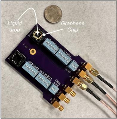
Graphene ISFET chip mounted on a printed circuit board (PCB). Image from: Nature

The sensor and AI can broadly detect and classify various substances while collectively assessing their respective quality, authenticity and freshness. This assessment has also provided the researchers with a view into how AI makes decisions, which could lead to better AI development and applications, they said.

Read the full story Posted: Oct 11,2024

Researchers investigate the ultrafast opto-electronic and thermal tuning of nonlinear optics in graphene

An international group of scientists, including ones from the UK's University of Bath, Friedrich Schiller University Jena in Germany and the University of Pisa in Italy, recently set out to investigate the ultrafast opto-electronic and thermal tuning of nonlinear optics in graphene.

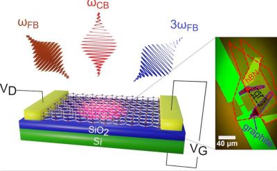
Opto-electronic modulation of third harmonic generation in a graphene field-effect transistor. The illustration includes a sketch and a microscopic optical image of the device. Image credit: University of Bath

Nonlinear optics explores how powerful light (e.g. lasers) interacts with materials, resulting in the output light changing color (i.e. frequency) or behaving differently based on the intensity of the incoming light. This field is important for developing advanced technologies such as high-speed communication systems and laser-based applications. Nonlinear optical phenomena enable the manipulation of light in novel ways, leading to breakthroughs in fields like telecommunications, medical imaging, and quantum computing. Graphene's exceptional electronic properties, related to relativistic-like Dirac electrons and strong light-matter interactions, make it promising for nonlinear optical applications, including ultrafast photonics, optical modulators, saturable absorbers in ultrafast lasers, and quantum optics.

Read the full story Posted: Oct 09,2024

Researchers combine graphene and silk for advanced microelectronics, wearables and next-gen computing applications

While silk protein has been used in designer electronics, its use is currently limited in part because silk fibers are a messy tangle of spaghetti-like strands. To address this, researchers from Pacific Northwest National Laboratory, University of Washington, Lawrence Berkeley National Laboratory, North Carolina State University and Xiamen University have developed a uniform two-dimensional (2D) layer of silk protein fragments, or "fibroins," on graphene. 

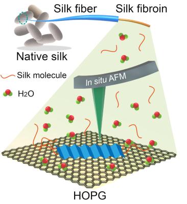
Scheme of silk fibroin assembly on highly oriented pyrolytic graphite (HOPG) characterized by in situ AFM. Image from Science Advances

The scientists explained that their work provides a reproducible method for silk protein self-assembly that is essential for designing and fabricating silk-based electronics. They said that the system is nontoxic and water-based, which is vital for biocompatibility.

Read the full story Posted: Sep 19,2024

Archer to test for chronic kidney disease on its Biochip gFET sensors

Archer Materials has started experiments to detect and monitor chronic kidney disease on its Biochip graphene field effect transistor (“gFET”) sensors.

Archer, through one of its foundry partners, has reportedly verified a process that directly grows graphene surfaces to produce enhanced devices, rather than transferring the graphene to a device from a wafer, as previously done. The team has tested the devices by storing them in normal air conditions over a two-month period, finding no significant degradation in performance. 

Read the full story Posted: Aug 31,2024

Graphene/germanium hot-emitter transistors could advance next-gen computing and communications technologies

Hot-carrier transistors are a class of devices that leverage the excess kinetic energy of carriers. Unlike regular transistors, which rely on steady-state carrier transport, hot-carrier transistors modulate carriers to high-energy states, resulting in enhanced device speed and functionality. These characteristics are essential for applications that demand rapid switching and high-frequency operations, such as advanced telecommunications and cutting-edge computing technologies. However, their performance has been limited by how hot carriers have traditionally been generated.

A team of researchers, led by Prof. Liu Chi, Prof. Sun Dongming, and Prof. CHeng Huiming from the Institute of Metal Research (IMR) of the Chinese Academy of Sciences, has proposed a novel hot carrier generation mechanism called stimulated emission of heated carriers (SEHC). The team has also developed an innovative hot-emitter transistor (HOET), achieving an ultralow sub-threshold swing of less than 1 mV/dec and a peak-to-valley current ratio exceeding 100. The study provides a prototype of a low power, multifunctional device for the post-Moore era.

Read the full story Posted: Aug 25,2024

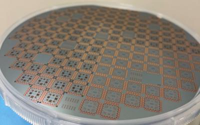
Archer Biochip gFET design fabricated on a six-inch wafer by Graphenea's foundry

Archer Materials, a semiconductor company advancing the quantum technology and medical diagnostics industries, has fabricated one of its Biochip graphene field effect transistor (gFET) designs through a six-inch whole wafer run by its foundry partner in Spain, Graphenea.

Archer had sent the Biochip gFET design to Graphenea for fabrication through a whole wafer run in Dec 20231. The gFETs are designed with structures suitable for liquid multiplexing, with advances in chip design features, including in gating design and materials, to address technological challenges in maintaining graphene device stability from chip-to-chip.

Read the full story Posted: Jun 17,2024

Researchers show that electrons in double-layer graphene move like particles without any mass

Researchers from the University of Göttingen, Japan's National Institute for Materials Science and Massachusetts Institute of Technology (MIT) have demonstrated experimentally that electrons in naturally occurring double-layer graphene move like particles without any mass, in the same way that light travels. Furthermore, they have shown that the current can be "switched" on and off, which has potential for developing tiny, energy-efficient transistors. 

Among its many unusual properties, graphene is known for its extraordinarily high electrical conductivity due to the high and constant velocity of electrons travelling through this material. This unique feature has made scientists try to use graphene for faster and more energy-efficient transistors. The challenge has been that to make a transistor, the material needs to be controlled to have a highly insulating state in addition to its highly conductive state. In graphene, however, such a "switch" in the speed of the carrier cannot be easily achieved. In fact, graphene usually has no insulating state, which has limited graphene's potential a transistor.

Read the full story Posted: Apr 18,2024

Archer Materials miniaturizes biochip gFET chip design

Archer Materials has designed a miniaturized version of its Biochip graphene field effect transistor ("gFET") chip for fabrication at a commercial foundry.

The Archer Biochip contains a sensing region of which the gFET is the core component. Each gFET chip contains multiple gFETs, each of which is a transistor, which acts as a sensor. Archer has miniaturized the total chip size by redesigning the layout of the circuits creating these gFET transistors. The new miniaturized design has been sent to a foundry partner for a whole-wafer fabrication of reduced size gFET chips, which Archer intends to integrate with other parts of the Biochip technology.

Read the full story Posted: Mar 15,2024

Researchers use graphene to develop new metasurface architectures for ultrafast information processing and versatile terahertz sources

Traditional microelectronic architectures are currently used to power everything from advanced computers to everyday devices. However, scientists are always on the lookout for better technologies. Recently, Los Alamos National Laboratory scientists and their collaborators from Menlo Systems and Sandia National Laboratories, have designed and fabricated asymmetric, nano-sized gold structures on an atomically thin layer of graphene. The gold structures are dubbed “nanoantennas” based on the way they capture and focus light waves, forming optical “hot spots” that excite the electrons within the graphene. Only the graphene electrons very near the hot spots are excited, with the rest of the graphene remaining much less excited.

Illustration of an optoelectronic metasurface consisting of symmetry-broken gold nanoantennas on graphene. Image from Nature

The team adopted a teardrop shape of gold nanoantennas, where the breaking of inversion symmetry defines a directionality along the structure. The hot spots are located only at the sharp tips of the nanoantennas, leading to a pathway on which the excited hot electrons flow with net directionality — a charge current, controllable and tunable at the nanometer scale by exciting different combinations of hot spots. 

Read the full story Posted: Feb 08,2024