While silk protein has been used in designer electronics, its use is currently limited in part because silk fibers are a messy tangle of spaghetti-like strands. To address this, researchers from Pacific Northwest National Laboratory, University of Washington, Lawrence Berkeley National Laboratory, North Carolina State University and Xiamen University have developed a uniform two-dimensional (2D) layer of silk protein fragments, or "fibroins," on graphene.
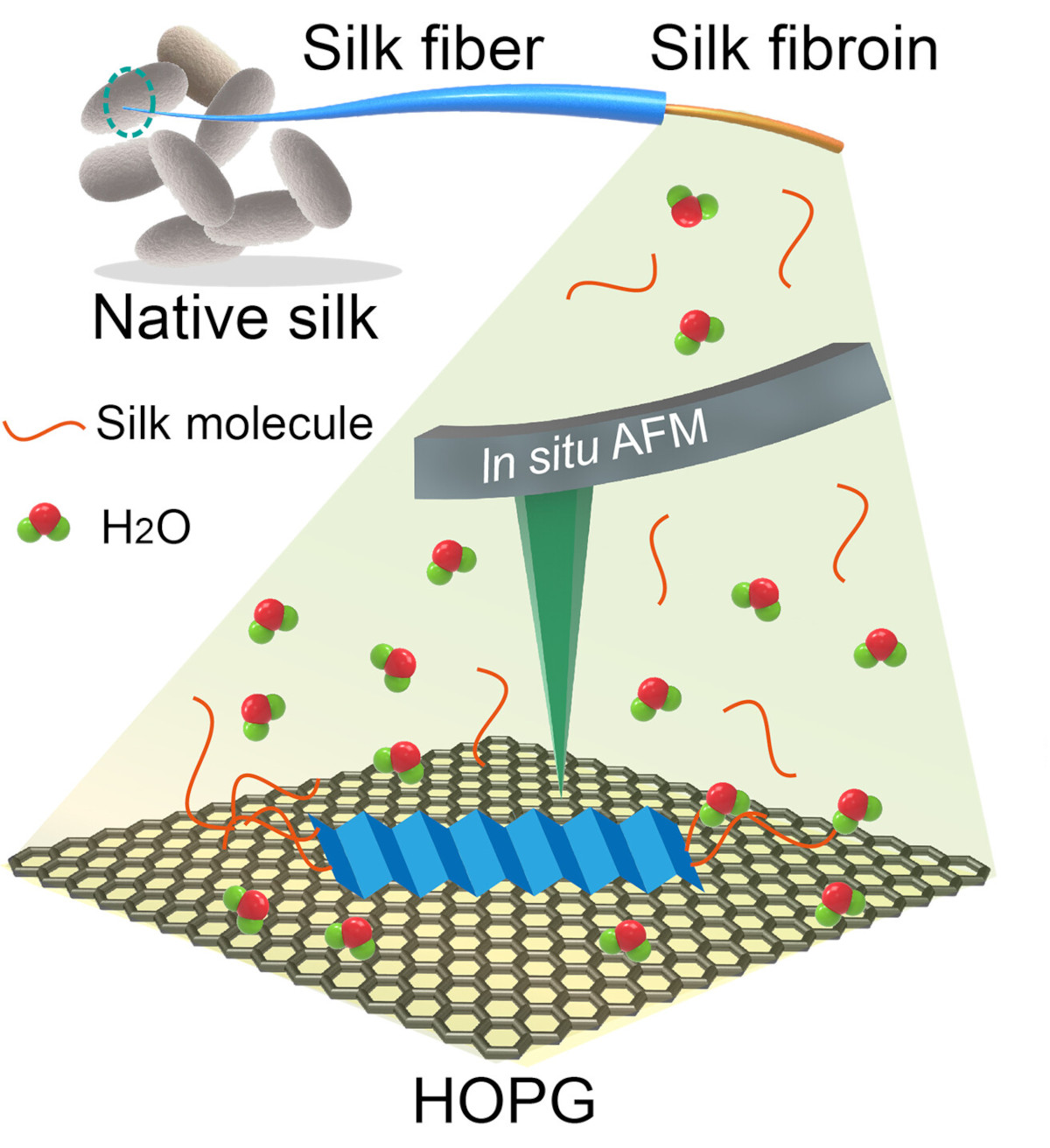
Scheme of silk fibroin assembly on highly oriented pyrolytic graphite (HOPG) characterized by in situ AFM. Image from Science Advances
The scientists explained that their work provides a reproducible method for silk protein self-assembly that is essential for designing and fabricating silk-based electronics. They said that the system is nontoxic and water-based, which is vital for biocompatibility.
This combination of materials - silk-on-graphene - could form a sensitive, tunable transistor highly desired by the microelectronics industry for wearable and implantable health sensors. The team also sees potential for their use as a key component of memory transistors or "memristors," in computing neural networks. Memristors, used in neural networks, allow computers to mimic how the human brain functions.
For many years, silk has been a status symbol and a coveted commodity associated with luxury. The same underlying properties that make silk fabric world-renowned, such as elasticity, durability, and strength, have led to its use in advanced materials applications.
According to the team, there's been a lot of research using silk as a way of modulating electronic signals, but since silk proteins are naturally disordered, there have been difficulties with achieving control. So, relying on the scientists' experience in controlling material growth on surfaces, they set out to make a better interface. To do that, the team carefully controlled the reaction conditions, adding individual silk fibers to the water-based system in a precise manner. Through precision laboratory conditions, the team achieved a highly organized 2D layer of proteins packed in precise parallel β-sheets, one of the most common protein shapes in nature. Further imaging studies and complementary theoretical calculations showed that the thin silk layer adopts a stable structure with features found in natural silk. An electronic structure at this scale - less than half the thickness of a strand of DNA - supports the miniaturization found everywhere in the bio-electronics industry.
"This type of material lends itself to what we call field effects," said James De Yoreo, who authored the study. "This means that it's a transistor switch that flips on or off in response to a signal. If you add, say, an antibody to it, then when a target protein binds, you cause a transistor to switch states."
The researchers are planning to use this starting material and technique to create their own artificial silk with functional proteins added to it to enhance its usefulness and specificity.
This study represents the first step in controlled silk layering on functional electronic components. Key areas of future research include improving the stability and conductivity of silk-integrated circuits and exploring silk's potential in biodegradable electronics to increase the use of green chemistry in electronic manufacturing.