Transistors - Page 4

Researchers design method to produce single-crystal graphene sheets on large-scale electrically insulating supports

Researchers from KAUST, Lanzhou University, Xiamen University, Friedrich Schiller University Jena and Ulsan have presented a method to produce single-crystal graphene sheets on large-scale electrically insulating supports. This approach could promote the development of next-generation nanomaterial-based devices, such as light and thin touchscreens, wearable electronics and solar cells.

Most graphene-based electronic devices require insulating supports. Yet, high-quality graphene films destined for industrial use are typically grown on a metal substrate, such as copper foil, before being transferred to an insulating support for device fabrication. This transfer step can introduce impurities that affect how well the device performs. Efforts to grow graphene on insulating supports have thus not been successful in producing the required high-quality single crystals.
Read the full story Posted: Apr 03,2022

INBRAIN Neuroelectronics signs an agreement to develop neurotechnology patented by six public research institutions

INBRAIN Neuroelectronics has signed an agreement for the exploitation and development of three patents and a trade secret, mainly held by the Institute of Microelectronics of Barcelona (IMB-CNM) of the Spanish Council for Scientific Research (CSIC), the Catalan Institute of Nanoscience and Nanotechnology (ICN2), the Institució Catalana de Recerca i Estudis Avançats (ICREA) and the Biomedical Research Centre Network CIBER BBN. The Universitat Autónoma de Barcelona (UAB) and the Institut de Investigacions Biomèdiques August Pi i Sunyer (IDIBAPS) are also co-owners of the patents. This is a successful process of technology transfer in a public-private collaboration with multiple research institutions.

The company will carry out the development and manufacturing of these technologies within the Institut Català de Nanociència i Nanotecnologia (ICN2) and the Micro and Nanofabrication Clean Room of the Institute of Microelectronics of Barcelona (IMB-CNM) of the CSIC.


Read the full story Posted: Mar 15,2022

Researchers create miniscule graphene-MoS2 transistors

Researchers from China's Tsinghua University and East China Normal University have created a transistor with the smallest gate length ever reported. This milestone was made possible by using graphene and molybdenum disulfide and stacking them into a staircase-like structure with two steps.

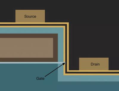
Vertical MoS2 transistors with sub-1-nm gate lengths imageThe structure of the side-wall transistor: Silicon dioxide base (dark blue), aluminum covered in aluminum oxide (brown ), the thin, light blue strip is graphene, the yellow and black strip is molybdenum disulfide, and underneath it, the hafnium dioxide.

On the higher step, there is the source, and on top of the lower step, there is the drain. Both are made of a titanium palladium alloy separated by the surface of the stairs, which is made of a single sheet of a molybdenum disulfide (MoS2), itself resting on a layer of hafnium dioxide that acts as an electrical insulator.

Read the full story Posted: Mar 15,2022

Researchers design a graphene-based sensor that can detect opioids in wastewater

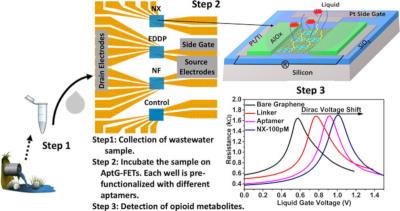
Researchers from Boston College, Boston University, and Giner Labs have designed a small graphene-based multiplexed bio-sensor that detects opioid byproducts in wastewater.

Graphene sensor rapidly detects opioids in wastewater image

The novel device uses graphene-based field effect transistors to detect four different synthetic and natural opioids at once, while shielding them from wastewater’s harsh elements. When a specific opioid metabolite attaches to a molecular probe on the graphene, it changes the electrical charge on the graphene. These signals are easily read electronically for each probe attached to the device.

Read the full story Posted: Feb 27,2022

New graphene-based neural probes improve detection of epileptic brain signals

Researchers the UK and Spain have demonstrated that tiny graphene neural probes can be used safely to improve our understanding of the causes of epilepsy.

The graphene depth neural probe (gDNP) consists of a millimeter-long linear array of micro-transistors imbedded in a micrometer-thin polymeric flexible substrate. The transistors were developed by a collaboration between The University of Manchester’s Neuromedicine Lab and UCL’s Institute of Neurology along with their Graphene Flagship partners.

Read the full story Posted: Dec 26,2021

Researchers demonstrate Doppler effect and sonic boom in graphene devices

A team of researchers from universities in Loughborough, Nottingham, Manchester, Lancaster and Kansas (US) has revealed that sonic boom and Doppler-shifted sound waves can be created in a graphene transistor.

When a police car speeds past you with its siren blaring, you hear a distinct change in the frequency of the siren’s noise. This is the Doppler effect. When a jet aircraft’s speed exceeds the speed of sound (about 760 mph), the pressure it exerts upon the air produces a shock wave which can be heard as a loud supersonic boom or thunderclap. This is the Mach effect. The scientists discovered that a quantum mechanical version of these phenomena occurs in an electronic transistor made from high-purity graphene.

Read the full story Posted: Nov 09,2021

Combining graphene transistors with MOFs yields selective and sensitive sensors

Karlsruhe Institute Of Technology (KIT) and Technical University of Darmstadt researchers have developed graphene-enhanced sensors for molecules in the gas phase. The functional principle of this new type of sensors is based on sensitive graphene transistors and tailor-made organometallic coatings. This combination enables selective detection of molecules.

Process flow of graphene MOFs sensors imageFabrication of SURMOF/GFET process flow. Image from article

As a prototype, the authors of the new study demonstrated a specific ethanol sensor that, unlike currently available commercial sensors, does not react to other alcohols or moisture.

Read the full story Posted: Sep 13,2021

Researchers succeed in creating single-crystal, large-area, fold-free monolayer graphene

A team of researchers, led by Director Rod Ruoff at the Center for Multidimensional Carbon Materials (CMCM) within the Institute for Basic Science (IBS) and including graduate students at the Ulsan National Institute of Science and Technology (UNIST), has achieved growth and characterization of large area, single-crystal graphene totally free from wrinkles, folds, or adlayers. It was said to be 'the most perfect graphene that has been grown and characterized, to date'.

Director Ruoff notes: This pioneering breakthrough was due to many contributing factors, including human ingenuity and the ability of the CMCM researchers to reproducibly make large-area single-crystal Cu-Ni(111) foils, on which the graphene was grown by chemical vapor deposition (CVD) using a mixture of ethylene with hydrogen in a stream of argon gas. Student Meihui Wang, Dr. Ming Huang, and Dr. Da Luo along with Ruoff undertook a series of experiments of growing single-crystal and single-layer graphene on such ‘home-made’ Cu-Ni(111) foils under different temperatures.

Read the full story Posted: Aug 27,2021

Graphenea Foundry: a platform for the manufacture of graphene-based devices

This is a sponsored post by Graphenea

Graphenea’s Semiconductor catalogue spans from 1x1 cm2 single layer graphene films on a variety of substrates, to fully customized graphene-based device architectures implemented on wafers up to 150mm. The unique vertical integration that Graphenea offers, that covers the graphene growth, its transfer, its device fabrication and post-processing, allows Graphenea to have full control of the manufacturing process, continuously monitoring this through quality control processes and checkpoints.

GFET wafers (Graphenea)

Graphenea Foundry offers three products and services, which cover all the graphene needs one may have.

Read the full story Posted: Aug 17,2021