Transistors - Page 5

Graphene-diamond junctions could assist in the realization of neuromorphic optical computers simulating human visual memory systems

Researchers from Nagoya University in Japan have designed highly efficient computing devices using graphene-diamond junctions that mimic some of the human brain's functions.

Schematics of optoelectronic synaptic functions of vertically aligned graphene/diamond junctions image

A phenomenon crucial for memory and learning is "synaptic plasticity," the ability of synapses (neuronal links) to adapt in response to increased or decreased activity. Scientists have tried to recreate a similar effect using transistors and "memristors" (electronic memory devices whose resistance can be stored). Recently developed light-controlled memristors, or "photomemristors," can both detect light and provide non-volatile memory, similar to human visual perception and memory. These excellent properties have opened the door to new materials that can act as artificial optoelectronic synapses.

Read the full story Posted: Aug 04,2021

Cardea Bio partners with Scentian Bio to create a bio-electronic tongue/nose platform

Cardea Bio, a biotech company integrating molecular biology with semiconductor electronics, has signed a commercial partnership with Scentian Bio. Scentian is an expert in synthetic insect odorant receptors (iORs), one of nature’s ways of detecting and interpreting smells.

The partnership will enable Scentian to use a customized Cardean chipset, built with graphene-based biology-gated transistors, which will allow Scentian to manufacture a bio-electronic tongue/nose tech platform.

Read the full story Posted: May 18,2021

Researchers show that the terahertz nonlinearity of graphene can be efficiently controlled using minimal electrical gating

A team of researchers from Bielefeld and Berlin, together with researchers from other research institutes in Germany and Spain, recently demonstrated that graphene's nonlinearity can be efficiently controlled by applying comparatively modest electrical voltages to the material.

The gated graphene sample device in which the graphene film acts as a channel between source and drain electrodes  imageThe gated graphene sample device in which the graphene film acts as a channel between source and drain electrodes subjected to a constant potential difference of 0.2 mV. Image from Science Advances

It was recently discovered that the high electronic conductivity and "massless" behavior of graphene's electrons allows it to alter the frequency components of electric currents that pass through it. This property is highly dependent on how strong this current is. In modern electronics, such a nonlinearity comprises one of the most basic functionalities for switching and processing of electrical signals. What makes graphene unique is that its nonlinearity is by far the strongest of all electronic materials. Moreover, it works very well for exceptionally high electronic frequencies, extending into the technologically important terahertz (THz) range where most conventional electronic materials fail.

Read the full story Posted: Apr 15,2021

Cardea Bio and the Georgia Tech Research Institute enter DARPA agreement to develop airborne SARS-CoV-2 sensors

The Defense Advanced Research Projects Agency (DARPA) recently awarded the Georgia Tech Research Institute (GTRI) an agreement, as part of their SenSARS program, to develop a sensing platform to detect airborne SARS-CoV-2 particles. Cardea Bio is a sub-contractor to this agreement.

This agreement will enable the two institutions to develop a real-time pathogen identification technology that can be applied to many different defense and civilian environmental monitoring applications.

Read the full story Posted: Mar 05,2021

Graphene ‘nano-origami’ could enable tiny microchips

Scientists at the University of Sussex have developed a technique for making tiny microchips from graphene and other 2D materials, using a form of ‘nano-origami’.

By creating distortions in the structure of the graphene, the researchers were able to make the nanomaterial behave like a transistor. We’re mechanically creating kinks in a layer of graphene, says Professor Alan Dalton of the School of Mathematical and Physics Sciences at the University of Sussex. It’s a bit like nano-origami. Using these nanomaterials will make our computer chips smaller and faster. It is absolutely critical that this happens as computer manufacturers are now at the limit of what they can do with traditional semiconducting technology. Ultimately, this will make our computers and phones thousands of times faster in the future.

Read the full story Posted: Feb 16,2021

Researchers design an accurate, high-speed, portable bifunctional electrical detector for COVID-19

A research team at South China University of Technology, Peking University and other China-based universities have developed an accurate, rapid, and portable electrical detector based on the use of graphene field-effect transistors (G-FETs) for detection of RNA from COVID-19 patients.

Schematic diagram of the operation procedure of our G-FET-based biosensing system for COVID-19 image

The detection system consists of two main parts: a plug-and-play packaged biosensor chip and an electrical measurement machine. The unique feature of this method is that the extent of hybridization between the ss-DNA probe and viral RNA can be directly converted to the current change of graphene channels without repetition of the PCR process. Furthermore, this method was validated using clinical samples collected from many patients with COVID-19 infection and healthy individuals as well, and the testing results were in full agreement with those of PCR-based optical methods.

Read the full story Posted: Jan 26,2021

Researchers design method that makes graphene nanoribbons easier to produce

Russian researchers have proposed a new method for synthesizing high-quality graphene nanoribbons. The team's approach to chemical vapor deposition offers a higher yield at a lower cost, compared with the currently used nanoribbon self-assembly on noble metal substrates.

Two nanoribbon edge configurations imageTwo nanoribbon edge configurations. The pink network of carbon atoms is a ribbon with zigzag (Z) edges, and the yellow one has so-called armchair (A) edges. Image credit MIPT

Unlike silicon, graphene does not have the ability to switch between a conductive and a nonconductive state. This defining characteristic of semiconductors is crucial for creating transistors, which are the basis for all of electronics. However, once you cut graphene into narrow ribbons, they gain semiconducting properties, provided that the edges have the right geometry and there are no structural defects. Such nanoribbons have already been used in experimental transistors with reasonably good characteristics, and the material’s elasticity means the devices can be made flexible. While it is technologically challenging to integrate 2D materials with 3D electronics, there are no fundamental reasons why nanoribbons could not replace silicon.

Read the full story Posted: Jan 12,2021

A new project called GraphCAT will aim to create an ecosystem of graphene research

A new project was recently launched under the name of GraphCAT, an initiative to create an ecosystem of research centers focused in the study of graphene. The project received funding from the Government of Catalonia and the European Union.

The ultimate vision of the GraphCAT Community is to establish Catalonia as an international hub for graphene research, development and innovation, with multiple local industries deriving strong competitive advantage in the global marketplace through the integration of proprietary graphene technologies into their products and services.

Read the full story Posted: Nov 21,2020

Researchers examine novel inkjet-printed graphene for high‐quality large‐area electronics

Researchers from the University of Nottingham’s Centre for Additive Manufacturing (CfAM) have reported a breakthrough in the study of 3D printing electronic devices with graphene.

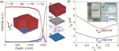
inkjet‐printed graphene/hBN FET imageCharacterization of the fully inkjet‐printed graphene/hBN FET. Photo from article

The scientists utilized an inkjet-based 3D printing technique to deposit inks that contained flakes of graphene, in a promising step towards replacing single-layer graphene as a contact material for 2D metal semiconductors.

Read the full story Posted: Nov 09,2020

Graphene nano-ribbons could help build future integrated circuits

University of California researchers, along with teams from other U.S-based institutions like Columbia University, Lawrence Berkeley National Laboratory and University of Washington, have created a metallic wire made entirely of carbon, setting the stage for a ramp-up in research to build carbon-based transistors and, ultimately, computers.

"Staying within the same material, within the realm of carbon-based materials, is what brings this technology together now," said Felix Fischer, UC Berkeley professor of chemistry, noting that the ability to make all circuit elements from the same material makes fabrication easier. "That has been one of the key things that has been missing in the big picture of an all-carbon-based integrated circuit architecture."

Read the full story Posted: Sep 25,2020