Electronics - Page 21

Graphene's lubricity to enable frictionless coatings

An international collaboration of scientists from the University of Basel and the Swiss Empa have studied the above-average lubricity of graphene using a two-pronged approach combining experimentation and computation. The researchers state that the results of this study help them to better understand the manipulation of chemicals at the nano level and pave the way for creating frictionless coatings.
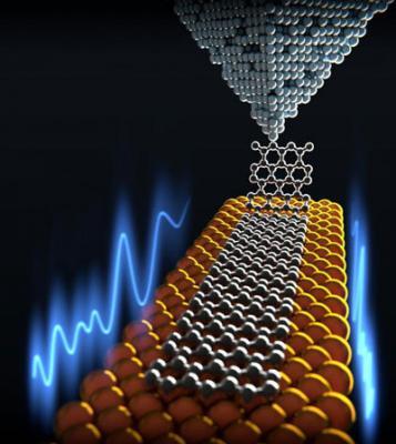
To do this, they anchored 2D strips of carbon atoms (graphene nanoribbons) to a sharp tip and dragged them across a gold surface. Computer-based calculations were used to investigate the interactions between the surfaces as they moved across one another. Using this approach, the research team hoped to gain a better understanding of the causes of superlubricity.

Read the full story Posted: Mar 01,2016

New hexagonal 2D material may rival graphene

Researchers from the University of Kentucky working in collaboration with scientists from Daimler in Germany and the Institute for Electronic Structure and Laser (IESL) in Greece have reported a new (theoretical) 2D material that could potentially rival graphene as the material of the future. The new material is made up of silicon, boron and nitrogen — all light, inexpensive and abundant elements — and is extremely stable, a property many other graphene alternatives lack.

While there are many ways to combine silicon, boron and nitrogen to form planar structures, only one specific arrangement of these elements resulted in a stable structure. The atoms in the new structure are arranged in a hexagonal pattern, as in graphene. The three elements forming the material all have different sizes; the bonds connecting the atoms are also different. As a result, the sides of the hexagons formed by these atoms are unequal, unlike in graphene.

Read the full story Posted: Feb 29,2016

Promising graphene-based component achieved using a new, simple method

Researchers at Aalto University in Finland have fabricated an electricity-conducting material with promising properties by merging graphene and another 2D material, gallium selenide. The newly designed heterojunction could prove important for applications like sensors and wearable electronics and are, in comparison similar components that contain silicon, extremely thin. They also have impressive properties and the method used for their preparation is simpler than previous researched methods.

The component structure utilized elements from both lateral and vertical device design enabling the use of standard fabrication methods utilized in the semiconductor industry instead of laborious manual fabrication. The scientists explain that their inspiration comes from the existing silicon technology, aiming to bring out the state-of-the-art fabrication of 2D material devices from research labs to industry. In addition to the new and simpler way of manufacturing, the components have excellent characteristics like the on/off ratio, which is a critical parameter in electronics - over 10³.

Read the full story Posted: Feb 21,2016

CPI's Graphene Centre now open for business

The Centre for Process Innovation (CPI) has opened the doors of a Graphene Centre that aims to help companies develop, prove and commercialize products using graphene technologies. The Graphene Centre was funded by Innovate UK to support the commercial growth of the UK graphene industry and operates two specialized facilities at NETPark in Sedgefield, County Durham.

It has a dedicated laboratory for the functionalization and characterization of Graphene at a significant scale, which is produced by a variety of process routes. The second facility is based in CPI’s printable electronics facility and is focused on device development and testing covering membranes, sensors, energy and electronic applications.

Read the full story Posted: Feb 18,2016

Graphene achieves superconductivity

A collaborative team from Tohoku University and the University of Tokyo has designed a way to make graphene superconductive, which means electrons can flow through it with zero resistance. This can lead to significantly more efficient electronic devices, power lines, high-speed electronic devices and more.

While exciting, it is important to say that this demonstration of superconductivity in graphene occurred at a temperature of -269 degrees Celsius, and room temperature superconductivity is still far from attainable. However, this research does suggest that graphene could be used to build nano-sized, high-speed electronic devices.

Read the full story Posted: Feb 17,2016

Interaction between graphene and glass may advance electronics and solar cells

A collaborative team of scientists from the U.S. Department of Energy's (DOE) Brookhaven National Laboratory, Stony Brook University (SBU), and the Colleges of Nanoscale Science and Engineering at SUNY Polytechnic Institute have developed a simple method for creating resilient, customized, and high-performing graphene: layering it on top of common glass. The scalable and inexpensive process may help pave the way for a new class of microelectronic and optoelectronic devices-from efficient solar cells to touch screens.

The team designed the proof-of-concept graphene devices on substrates made of soda-lime glass-the most common glass found in windows, bottles, and many other products. Unexpectedly, the sodium atoms in the glass had a powerful effect on the electronic properties of the graphene - it created high electron density in the graphene, which is essential to many processes and has been challenging to achieve. Also, the effect remained strong even when the devices were exposed to air for several weeks- a clear improvement over competing techniques.

Read the full story Posted: Feb 14,2016

Wrapping graphene oxide around copper nanowires improves its stability in air

Researchers at the University of California at Berkeley and the Lawrence Berkeley National Laboratory have developed a new solution-based, cost-effective way to wrap reduced graphene oxide around the surface of ultrathin transparent conducting copper nanowires. The technique aims to significantly improve the stability of the wires in air and reduce the amount of light scattered by the materials.

Thin films made of the wires might be used in optoelectronics devices, particularly in displays and flexible electronics. Metal nanowire films could make good replacements for the expensive and brittle indium tin oxide (ITO) in next-generation electronics, thanks to their excellent electrical and optical properties and the fact that they can be easily processed in solution.

Read the full story Posted: Feb 09,2016 - 1 comment

Printed graphene oxide makes for interesting electronic devices

Researchers at the Barcelona Institute of Science and Technology have managed to print graphene oxide onto different materials, including paper, and use it as a touch sensitive electronic device. They transferred graphene oxide coated on a wax printed membrane to paper, an adhesive film and even a t-shirt by simply using pressure and water, and also printed graphene oxide onto plastic and, as the oxide conducts electricity, used it as a touch sensitive LED switch.

 
Read the full story Posted: Jan 25,2016

New facility for graphene manufacture and R&D launched by The University of Granada

The University of Granada in Spain has launched the Graphene and 2D Semiconductors Laboratory, said to be one of the most complete public laboratories devoted to the manufacture and electric and structural characterization of graphene in Europe. This laboratory is supposedly comparable to that of the University of Cambridge (United Kingdom) or the one in the University of Stanford (United States).

The new facilities are located in the UGR Research Centre for Information Technology and Communication. With an investment of more than half a million euros, the new laboratory is devoted to the manufacture of all kinds and forms of graphene as well as the development of new graphene-based systems for electronic applications which include biosensors, electronic nanodevices for IoT (Internet of Things) applications, and flexible electronics, in addition to wearable devices.

Read the full story Posted: Jan 22,2016

Graphene oxide's reaction to strain may enable many next-gen applications

Researchers at Rice University and the State University of Campinas in Brazil have found that random molecules scattered within layers of otherwise pristine graphene affect how the layers interact with each other under strain. The researchers, with flexible electronics in mind, decided to see how graphene oxide paper would handle shear strain, in which the sheets are pulled by the ends. Such knowledge is important for applications involving novel advanced materials, especially for making 3D structures from 2D materials, and some applications may include sensors, electronics and biomedical devices. 

Read the full story Posted: Jan 22,2016