Electronics - Page 10

Superconductivity in bilayer graphene can be turned on or off with a voltage change

An international team of researchers from Spain, the U.S., China and Japan has found that superconductivity in bilayer graphene can be turned on or off with a small voltage change, increasing its usefulness for electronic devices. This follows previous findings regarding twisted bilayer graphene and its ability to exhibit alternating superconducting and insulating regions.

"It's kind of a holy grail of physics to create a material that has superconductivity at room temperature," University of Texas at Austin physicist Allan MacDonald said. "So that's part of the motivation of this work: to understand high-temperature superconductivity better."
Read the full story Posted: Nov 02,2019

Researchers reach graphene-based junctions that are both electrically and mechanically stable

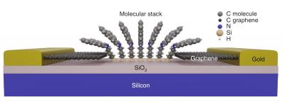
A research team jointly led by University of Warwick and EMPA has tackled a challenging issue of stability and reproducibility in working with graphene, that meant that graphene-based junctions were either mechanically stable or electrically stable but not both at the same time.

Researchers tackle a known limitation of graphene junctions imageCredit: University of Warwick

Graphene and graphene like molecules are attractive choices for electronic components in molecular devices, but have proven very challenging to use in large scale production of molecular devices that will work and be robust at room temperatures. The joint research team from the University of Warwick, EMPA and Lancaster and Bern Universities has reached both electrical and mechanical stability in graphene-based junctions.

Read the full story Posted: Sep 17,2019

Graphene and other 2D materials form an enhanced heat protector for electronics

Researchers from Stanford, NIST, Theiss Research and several others have designed a new heat protector that consists of just a few layers of atomically thin materials, to protect electronics from excess heat.

Cross-section schematic of Gr/MoSe2/MoS2/WSe2 sandwich on SiO2/Si substrate imageCross-section schematic of Gr/MoSe2/MoS2/WSe2 sandwich on SiO2/Si substrate, with the incident Raman laser

The heat protector can reportedly provide the same insulation as a sheet of glass 100 times thicker. We’re looking at the heat in electronic devices in an entirely new way, said Eric Pop, professor of electrical engineering at Stanford and senior author of the study.

Read the full story Posted: Aug 22,2019

End-to-end processing chain of 2D materials successfully demonstrated as part of project "HEA2D"

Project "HEA2D", which started in 2016 and set out to investigate the production, qualities, and applications of 2D nanomaterials, recently demonstrated end-to-end processing chain of two-dimensional nanomaterials. The project is a collaboration between AIXTRON, AMO, Coatema, Fraunhofer and Kunststoff-Institut für die mittelständische Wirtschaft (K.I.M.W.).

It was stated that the "HEA2D" consortium successfully demonstrated an end-to-end processing chain of two-dimensional nanomaterials as part of its results. 2D materials integrated into mass production processes have the potential to create integrated and systemic product and production solutions that are socially, economically and ecologically sustainable. Application areas for the technologies developed and materials investigated in this project are mainly composite materials and coatings, highly sensitive sensors, power generation and storage, electronics, information and communication technologies as well as photonics and quantum technologies.

Read the full story Posted: Jul 23,2019

Paragraf raises USD$16 million to push forward graphene-based electronics technologies

UK-based graphene technology company Paragraf has announced the close of its £12.8 million (over $16 million USD ) Series A round led by Parkwalk. The round also included investment from IQ Capital Partners, Amadeus Capital Partners and Cambridge Enterprise, the commercialization arm of the University of Cambridge, as well as several angel investors. The funding will aim to see Paragraf’s first graphene-based electronics products reach the market, transitioning the company into a commercial, revenue-generating entity.

Paragraf sets out to deliver IP-protected graphene technology using standard, mass production scale manufacturing approaches, enabling step-change performance enhancements to today’s electronic devices. The company’s first sensor products have reportedly demonstrated order of magnitude operational improvements over today’s incumbents. Achieving large-scale, graphene-based production technology may enable next generation electronics, including vastly increased computing speeds, significantly improved medical diagnostics and higher efficiency renewable energy generation as well as currently unachievable products such as instant charging batteries and very low power, flexible electronics.

Read the full story Posted: Jul 16,2019

Researchers discover new states of matter that arise from stacking 2D layers of graphene

Researchers from Brown and Columbia Universities in the U.S have demonstrated that unknown states of matter arise from stacking two-dimensional layers of graphene together. These new states have been named the fractional quantum Hall effect (FQHE), and are created through the complex interactions of electrons within and across graphene layers.

"In terms of materials engineering, this work shows that these layered systems could be viable in creating new types of electronic devices that take advantage of these new quantum Hall states," said Jia Li, assistant professor at Brown. Li added: "The findings show that stacking 2-D materials together in close proximity generates entirely new physics."

Read the full story Posted: Jul 04,2019

San Diego team creates LIG graphene composites for printed, stretchable wearables

Researchers at Joseph Wang's Laboratory for Nanobioelectronics at UC San Diego demonstrated the synthesis of high-performance stretchable graphene ink using a facile, scalable, and low-cost laser induction method for the synthesis of the graphene component.

The processing steps for screen-printed flexible supercapacitor fabricated from laser-induced graphene ink imageThe processing steps for screen-printed flexible supercapacitor fabricated from laser-induced graphene ink

As a proof-of-concept, the researchers fabricated a stretchable micro-supercapacitor (S-MSC) demonstrating high capacitance. This is said to be the first example of using laser-induced graphene in the form of a powder preparation of graphene-based inks and subsequently for use in screen-printing of S-MSC.

Read the full story Posted: Jun 19,2019

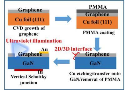
Understanding graphene/GaN and other 2D/3D interfaces by UV illumination could be crucial for next-gen electronics

Researchers from the Nagoya Institute of Technology (NITech) in Japan have developed a method to examine the connections between two-dimensional layers of atoms and semiconductors, which could prove useful in the future for ensuring the performance of next-gen electronics.

The fabrication process of vertical Schottky junction with monolayer graphene on free-standing GaN imageThe fabrication process of a monolayer graphene on free-standing GaN interface

The team applied a layer of graphene to gallium nitride, a commonly used semiconductor. The graphene is made of a single layer of atoms, while the gallium nitride is a three-dimensional structure. Together, graphene and gallium nitride are known as a heterojunction device, with significant sensitivity to the interface properties of metal and semiconductors.

Read the full story Posted: Jun 09,2019

Laser technique that opens a bandgap in graphene could allow for next-gen graphene electronics

Researchers from Purdue University, the University of Michigan and the Huazhong University of Science and Technology have used a technique called "laser shock imprinting" to permanently stress graphene into having a band gap, which could mean it would be possible to use it in various electronic components.

The researchers used a laser to create shock wave impulses that penetrated an underlying sheet of graphene. The laser shock stretches the graphene onto a permanent, trench-like mold. This caused the widening of band gap in graphene to a record 2.1 electronvolts. Previously, scientists achieved 0.5 electronvolts, barely reaching the benchmark to make graphene a semiconductor like silicon.

Read the full story Posted: Jun 02,2019

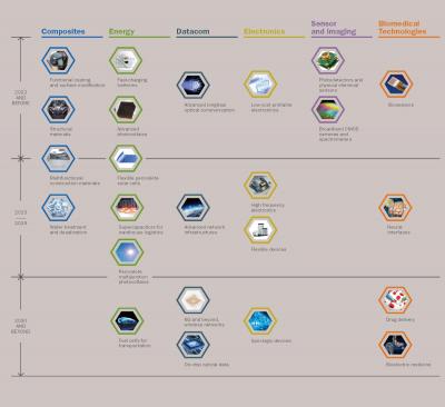
The Graphene Flagship announces its 2019-2030 graphene application roadmap

The EU Graphene Flagship has published its graphene application roadmap, showing when the flagship expects different graphene applications to mature and enter the market.

Graphene Flagship roadmap 2019-2030 photoAs can be seen in the roadmap above (click here for a larger image), the first applications that are being commercialized now are applications such as composite functional coatings, graphene batteries, low-cost printable electronics (based on graphene inks), photodetectors and biosensors.

Read the full story Posted: Apr 07,2019 - 4 comments