Electronics - Page 9

Researchers use graphene to create detachable flexible microLED devices

University of Texas at Dallas researchers and their international colleagues have developed a graphene-based method to create micro LEDs that can be folded, twisted, cut and stuck to different surfaces. The research could help pave the way for the next generation of flexible, wearable technology.
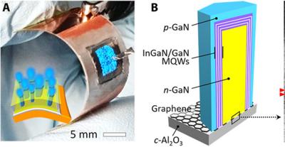
Graphene helps create flexible and detachable micro LEDs image(A) Photograph of EL light emission from MR LED in a bent form. (B) Cross-sectional schematic of MR heterostructures grown on graphene-coated c-Al2O3 wafer. Image from Science Advances

Used in various applications like signage and automotive lights, LEDs are ubiquitous because they are lightweight, thin, energy efficient and visible in different types of lighting. Micro LEDs, which can be as small as 2 micrometers and bundled to be any size, provide higher resolution than LEDs. Their size makes them a good fit for small devices such as smart watches, but they can be bundled to work in flat-screen TVs and other larger displays. LEDs of all sizes, however, are brittle and typically can only be used on flat surfaces. The researchers’ new micro LEDs aim to enable bendable, wearable electronics.
Read the full story Posted: Sep 01,2020

New graphene nanoribbons could enable smaller electronic devices

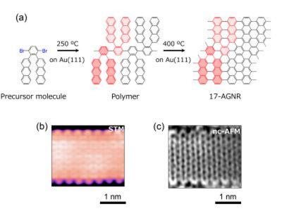
A new collaborative study has reported a 17-carbon wide graphene nanoribbon and found that it has the tiniest bandgap observed so far among familiar graphene nanoribbons prepared through a bottom-up approach.

17-carbon wide graphene nanoribbons to pave the way for new GNR-based electronic devices image(a) Bottom-up synthesis scheme of 17-AGNR on Au(111), (b) high-resolution STM image, and (c) nc-AFM image of 17-AGNR. Image Credit: Junichi Yamaguchi, Yasunobu Sugimoto, Shintaro Sato, Hiroko Yamada.

The study is part of a project of CREST, JST Japan including Nara Institute of Science and Technology (NAIST), the University of Tokyo, Fujitsu Laboratories and Fujitsu.

Read the full story Posted: Jul 06,2020

Researchers design a novel method for construction of van der Waals heterostructures using a dual-function polymeric film

A team of researchers has found a novel method for the construction of high-quality van der Waals (vdW) heterostructures, that are vital for many scientific studies and technological applications of layered materials. The work is a collaboration between the laboratory of Davood Shahrjerdi, a professor of Electrical and Computer Engineering at the NYU Tandon School of Engineering and a faculty member of NYU WIRELESS; a group led by Javad Shabani at the Center for Quantum Phenomena, New York University; and Kenji Watanabe and Takashi Taniguchi of National Institute for Materials Science, Japan.

Fabrication of vdW heterostructures image

A crucial step for building vdW graphene heterostructures is the production of large monolayer graphene flakes on a substrate, a process called mechanical exfoliation. The process then involves transferring the graphene flakes onto a target location for the assembly of the vdW heterostructure. An optimal substrate would therefore make it possible to efficiently and consistently exfoliate large flakes of monolayer graphene and subsequently release them on-demand for constructing a vdW heterostructure.

Read the full story Posted: Jun 16,2020

Stretchable Li-ion battery enhanced with graphene and CNTs to benefit wearable electronics

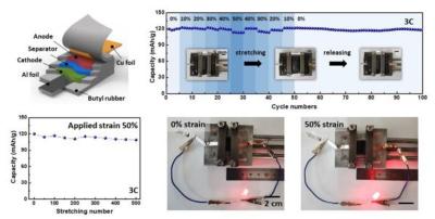
Scientists in the Korea Institute of Science and Technology (KIST) have worked with graphene and carbon nanotubes to develop a working lithium-ion battery that can be stretched by up to 50% without damage to any of the components. According to the scientists, the battery represents a significant step in the development of wearable or body-implantable electronic devices.

KIST team develops stretchable Li-ion battery with graphene and CNTs image

Rather than trying to add inherently stretchable materials such as rubber to the battery components, the group focused on creating an accordion-like structure, adding stretchability to materials that are not inherently stretchable. Using graphene and carbon nanotubes, the scientists were able to construct a honeycomb-shaped composite framework, which was then compressed inwardly like an accordion to impart the stretchable properties.

Read the full story Posted: May 03,2020

New grahene-based platform to open the door to various new applications

Penn State researchers, in conjunction with Lawrence Berkeley National Lab and Oak Ridge National Lab, have developed an atomically thin materials platform developed that could enable a range of new applications in biomolecular sensing, quantum phenomena, catalysis and nonlinear optics.

2D metals open pathways to new science imageA single atomic layer of metal is capped by a layer of graphene, allowing for new layered materials with unique properties. Image: Yihuang Xiong/Penn State

We have leveraged our understanding of a special type of graphene, dubbed epitaxial graphene, to stabilize unique forms of atomically thin metals, said Natalie Briggs, a doctoral candidate and co-lead author on a paper in the journal Nature Materials. Interestingly, these atomically thin metals stabilize in structures that are completely different from their bulk versions, and thus have very interesting properties compared to what is expected in bulk metals.

Read the full story Posted: Mar 10,2020

New method produces graphene on surfaces for precise electronics applications

Scientists at Rice University, the University of Tennessee, Knoxville (UT Knoxville) and Oak Ridge National Laboratory (ORNL) have demonstrated the use of a very small visible beam to burn graphene into microscopic patterns.

Schematic of the method for finely creating graphene with a small laser imageScientists recorded the formation of laser-induced graphene made with a small laser mounted to a scanning electron microscope. Image credit: the Tour Group

The labs of Rice chemist James Tour, which discovered the original method to turn a common polymer into graphene in 2014, and Tennessee/ORNL materials scientist Philip Rack revealed they can now watch the conductive material form as it makes small traces of LIG in a scanning electron microscope (SEM).

Read the full story Posted: Feb 13,2020

Special substrates enable large single crystal bi-/tri-layer graphene growth

Researchers of the Center for Multidimensional Carbon Materials (CMCM) within the Institute for Basic Science (IBS, South Korea), in collaboration with UNIST and Sungkyunkwan University teams, have reported the fabrication and use of single crystal copper-nickel alloy foil substrates for the growth of large-area, single crystal bilayer and trilayer graphene films.

The growth of large area graphene films with a precisely controlled number of layers and stacking order can open new possibilities in electronics and photonics but remains a challenge. This study showed an example of the synthesis of bi- and trilayer graphene sheets larger than a centimeter, with layers piled up in a specific manner, namely AB- and ABA-stacking.

Read the full story Posted: Jan 23,2020

New method uses hydrogen plasma to smooth out wrinkles in graphene

Researchers from Nanjing University in China have developed a method to make large graphene films free of any wrinkles. The ultra-smooth films could enable large-scale production of electronic devices that harness the unique physical and chemical properties of graphene and other 2D materials.

Wrinkles  disappear when graphene is treated with a hydrogen plasma imageWrinkles in graphene films grown via chemical vapor deposition appear as jagged white lines at the top of this atomic force microscope image (left), but they disappear when the material is treated with a hydrogen plasma (right). Credit: Nature

Chemical vapor deposition (CVD) is the best-known method for making high-quality graphene sheets. It typically involves growing graphene by pumping methane gas onto copper substrates heated to temperatures around 1,000 °C, and then transferring the graphene to another surface such as silicon. But some of the graphene sticks to the copper surface, and as the graphene and copper expand and contract at different rates, wrinkles form in the graphene sheets. Such wrinkles often present hurdles for charge carriers and lower the film’s conductivity. Other researchers have tried to reduce wrinkles using low growth temperatures or special copper substrates, but the wrinkles have proven difficult to eliminate entirely, according to Libo Gao, a physicist at Nanjing University.

Read the full story Posted: Jan 17,2020

Graphene enables researchers to visualize the flow of electrons

Researchers from Israel's Weizmann Institute and the UK's Manchester University have succeeded in imaging electrons' hydrodynamic flow pattern for the first time using a novel scanning probe technique. They have proven the longstanding scientific theory that electrons can behave like a viscous liquid as they travel through a conducting material, producing a spatial pattern that resembles water flowing through a pipe.

The results of this study could help developers of future electronic devices, especially those based on 2D materials like graphene in which electron hydrodynamics is important.

Read the full story Posted: Dec 12,2019

Graphenea launches highly flat monolayer graphene on copper thin film

Graphenea has announced the launch of a new product highly flat monolayer graphene. The graphene is grown by CVD on copper thin film on a 2 sapphire substrate. With extremely low roughness that is less than 4 nm, this new product is targeted at applications in photonics, high-performance electronics, magnetic memory, and freestanding membranes.

Graphenea's new flat monolayer graphene on copper thin film image

The product aims to meet wafer-scale integration requirements to build uniform graphene devices in a fashion compatible with current industrial fabrication methods. The flat graphene product is ready to be transferred by electrochemical delamination or dry methods since the sapphire substrate is robust enough to withstand mechanical damage, preventing tearing and wrinkling of the thin Cu sheet. The total wafer thickness is 430 micrometers. Full product information can be found in Graphenea's online store.

Read the full story Posted: Dec 01,2019