Electronics - Page 8

Graphene ‘nano-origami’ could enable tiny microchips

Scientists at the University of Sussex have developed a technique for making tiny microchips from graphene and other 2D materials, using a form of ‘nano-origami’.

By creating distortions in the structure of the graphene, the researchers were able to make the nanomaterial behave like a transistor. We’re mechanically creating kinks in a layer of graphene, says Professor Alan Dalton of the School of Mathematical and Physics Sciences at the University of Sussex. It’s a bit like nano-origami. Using these nanomaterials will make our computer chips smaller and faster. It is absolutely critical that this happens as computer manufacturers are now at the limit of what they can do with traditional semiconducting technology. Ultimately, this will make our computers and phones thousands of times faster in the future.

Read the full story Posted: Feb 16,2021

Researchers design method that makes graphene nanoribbons easier to produce

Russian researchers have proposed a new method for synthesizing high-quality graphene nanoribbons. The team's approach to chemical vapor deposition offers a higher yield at a lower cost, compared with the currently used nanoribbon self-assembly on noble metal substrates.

Two nanoribbon edge configurations imageTwo nanoribbon edge configurations. The pink network of carbon atoms is a ribbon with zigzag (Z) edges, and the yellow one has so-called armchair (A) edges. Image credit MIPT

Unlike silicon, graphene does not have the ability to switch between a conductive and a nonconductive state. This defining characteristic of semiconductors is crucial for creating transistors, which are the basis for all of electronics. However, once you cut graphene into narrow ribbons, they gain semiconducting properties, provided that the edges have the right geometry and there are no structural defects. Such nanoribbons have already been used in experimental transistors with reasonably good characteristics, and the material’s elasticity means the devices can be made flexible. While it is technologically challenging to integrate 2D materials with 3D electronics, there are no fundamental reasons why nanoribbons could not replace silicon.

Read the full story Posted: Jan 12,2021

Researchers develop monolayer graphene-based reversible self-folding structures

A team of scientists at Johns Hopkins University in the U.S. has designed a mass-production strategy to create monolayer graphene-based reversible self-folding structures. The material may find potential uses in microfluidics and micromechanical systems.

 Share  Email  Home Nanotechnology Nanophysics Home Nanotechnology Nanomaterials JANUARY 11, 2021 FEATURE  Self‐folding 3-D photosensitive graphene architectures imageMechanism and versatility of self‐folding SU8 films. Image from article

As proof of concept, the team achieved complex and functional devices in the form of rings, polyhedra, flowers and origami birds. They then integrated gold electrodes to the constructs to improve their detection sensitivity. The experiments suggest a comprehensive framework to rationally design and fabricate scalable and complex, 3D, self-folding optical and electronic devices by folding 2D monolayer graphene.

Read the full story Posted: Jan 12,2021

Researchers design a novel method for modifying the structure and properties of graphene

An international research team from China, France, Canada, Denmark and the UK has demonstrated a novel process to modify the structure and properties of graphene. This chemical reaction, known as photocycloaddition, modifies the bonds between atoms using ultraviolet light.

A new method for the functionalization of graphene image

The researchers demonstrated a spatially selective photocycloaddition reaction of a two-dimensional molecular network with defect-free basal plane of single-layer graphene. The cycloaddition is triggered by ultraviolet irradiation in ultrahigh vacuum, requiring no aid of the graphene Moiré pattern. This work could open the door to designing and engineering graphene-based optoelectronic and microelectronic devices.

Read the full story Posted: Dec 16,2020

International team develops novel method to modify the structure and properties of graphene

An international research team, that included researchers from the Harbin Institute of Technology in China, INRS in France and more, has demonstrated a novel process to modify the structure and properties of graphene. This process relied on a chemical reaction known as photocycloaddition, that modifies the bonds between atoms using ultraviolet (UV) light.

Photocycloaddition of the BCM layer with graphene image

"No other material has properties similar to graphene, yet unlike semiconductors used in electronics, it lacks a band gap. In electronics, this gap is a space in which there are no energy levels that can be occupied by electrons. Yet it is essential for interacting with light," explains Professor Federico Rosei of INRS's Énergie Matériaux Télécommunications Research Centre.

Read the full story Posted: Dec 16,2020

Researchers design a lightweight and highly efficient graphene heat pipe

Researchers at Sweden-based Chalmers University of Technology, in collaboration with researchers in China and Italy, have found that graphene-based heat pipes can help solve the problems of cooling electronics and power systems used in avionics, data centers, and other power electronics.

Cooling electronics efficiently with graphene-enhanced heat pipes imageA) Image of a real GHP; B) schematic designing of the GHP; C) working principle of the GHP

Electronics and data centers need to be efficiently cooled and rid of excess heat in order to function properly. Currently, heat pipes are usually made of copper, aluminum or their alloys. Due to the relatively high density and limited heat transmission capacity of these materials, heat pipes are facing severe challenges in future power devices and data centers.

Read the full story Posted: Dec 03,2020

Paragraf, Rolls-Royce, TT Electronics and the Compound Semiconductor Applications Catapult join to establish a first-ever supply chain for graphene Hall Effect sensors

Paragraf, UK-based graphene electronic sensors and devices company, announced that it is helping to realize an industry first by implementing a supply chain for graphene Hall-Effect sensors used in high-temperature Power Electronics, Electric Machines and Drives (PEMD) within the aerospace sector.

Paragraf graphene Hall Effect sensors image

Named High-T Hall, the project stems from the UK Research and Innovation’s (UKRI) ‘Driving the Electric Revolution’ challenge and brings together Paragraf, Rolls-Royce, TT Electronics (Aero Stanrew) and the Compound Semiconductor Applications Catapult (CSA Catapult). It is set to demonstrate how graphene-based Hall Effect sensors can operate reliably at high temperatures, paving the way for more efficient electric engines in aerospace and beyond.

Read the full story Posted: Dec 02,2020

Researchers examine novel inkjet-printed graphene for high‐quality large‐area electronics

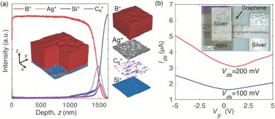
Researchers from the University of Nottingham’s Centre for Additive Manufacturing (CfAM) have reported a breakthrough in the study of 3D printing electronic devices with graphene.

inkjet‐printed graphene/hBN FET imageCharacterization of the fully inkjet‐printed graphene/hBN FET. Photo from article

The scientists utilized an inkjet-based 3D printing technique to deposit inks that contained flakes of graphene, in a promising step towards replacing single-layer graphene as a contact material for 2D metal semiconductors.

Read the full story Posted: Nov 09,2020

Researchers design graphene-based broadband detector of terahertz radiation

Scientists from Russia and Germany have created a graphene-based broadband detector of terahertz radiation. The device could have potential for applications in communication and next-generation information transmission systems, security and medical equipment.

Graphene detector reveals THz light’s polarization image(a) shows a top view of the device, with the sensitive region magnified in (b). The labels S, D, and TG denote the source, drain, and top gate. A side section of the detector is shown in (c). Image from MIPT

The new detector relies on the interference of plasma waves. Plasma waves in metals and semiconductors have recently attracted much attention from researchers around the world. Like the more familiar acoustic waves, the ones that occur in plasmas are essentially density waves, too, but they involve charge carriers: electrons and holes. Their local density variation gives rise to an electric field, which nudges other charge carriers as it propagates through the material. This is similar to how the pressure gradient of a sound wave impels the gas or liquid particles in an ever expanding region. However, plasma waves die down rapidly in conventional conductors.

Read the full story Posted: Oct 15,2020

Researchers track the path of calcium atoms added to graphene

Researchers from Australia's Monash University, U.S Naval Research Laboratory, University of Maryland and IMDEA Nanociencia in Spain have confirmed what actually happens to calcium atoms that are added to graphene in order to create a superconductor: surprisingly, the calcium goes underneath both the upper graphene sheet and a lower ‘buffer’ sheet, ‘floating’ the graphene on a bed of calcium atoms.

Injecting calcium into graphene creates a superconductor, but where does the calcium actually end up image

Superconducting calcium-injected graphene holds great promise for energy-efficient electronics and transparent electronics.

Read the full story Posted: Sep 17,2020